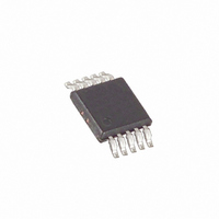
MAX9924UAUB+ Maxim Integrated Products, MAX9924UAUB+ Datasheet - Page 14

MAX9924UAUB+
Manufacturer Part Number
MAX9924UAUB+
Description
IC SENSOR INTERFACE VARI 10MSOP
Manufacturer
Maxim Integrated Products
Type
Sensor Interfacer
Datasheet
1.MAX9927AEE.pdf
(23 pages)
Specifications of MAX9924UAUB+
Input Type
Differential
Output Type
Logic
Interface
Differential
Current - Supply
5mA
Mounting Type
Surface Mount
Package / Case
10-MSOP, Micro10™, 10-uMAX, 10-uSOP
Lead Free Status / RoHS Status
Lead free / RoHS Compliant
Variable Reluctance Sensor Interfaces with
Differential Input and Adaptive Peak Threshold
The zero-crossing signal provides true timing informa-
tion for engine-control applications. The zero-voltage
level in the VR sensor signal corresponds to the center
of the gear-tooth and is the most reliable marker for
position/angle-sensing applications. Since the output of
the differential amplifier is level-shifted to the BIAS volt-
age, the zero of the input VR signal is simply BIAS. The
comparator output state controls the status of the input
switch that changes the voltage at its noninverting input
from the adaptive/external threshold level to the BIAS
level. The difference in these two voltages then effec-
tively acts as hysteresis for the comparator, thus pro-
viding noise immunity.
The internal comparator is a fast open-drain output
comparator with low input offset voltage and drift. The
comparator precision affects the ability of the signal
chain to resolve small VR sensor signals. An open-drain
output allows the comparator to easily interface to a
variety of µC I/O voltages.
When operating the MAX9924/MAX9925/MAX9926 in
Mode C, external hysteresis can be provided by adding
external resistors (see Figures 5 and 8). The high and
low hysteresis thresholds in Mode C can be calculated
using the following equations,
and
14
______________________________________________________________________________________
V
TH
=
⎛
⎜
⎝
V
R V
TL
1
R
(
1
=
+
PULLUP
⎛
⎜
⎝
R
R
2
1
+
R
+
R
2
R
PULLUP
2
−
⎞
⎟ ×
⎠
V
BIAS
V
BIAS
)
Zero Crossing
⎞
⎟ +
⎠
Comparator
V
BIAS
For quadrature-connected VR sensors, the open-drain
output DIRN indicates the rotational direction of inputs
IN1 and IN2 based on the output state of COUT1 and
COUT2. DIRN goes high when COUT1 is leading
COUT2, and low when COUT1 is following COUT2.
Good power-supply decoupling with high-quality
bypass capacitors is always important for precision
analog circuits. The use of an internal charge pump for
the front-end amplifier makes this more important.
Bypass capacitors create a low-impedance path to
ground for noise present on the power supply.
The minimum impedance of a capacitor is limited to the
effective series resistance (ESR) at the self-resonance
frequency, where the effective series inductance (ESL)
cancels out the capacitance. The ESL of the capacitor
dominates past the self-resonance frequency resulting
in a rise in impedance at high frequencies.
Bypass the power supply of the MAX9924–MAX9927
with multiple capacitor values in parallel to ground. The
use of multiple values ensures that there will be multiple
self-resonance frequencies in the bypass network, low-
ering the combined impedance over frequency. It is
recommended to use low-ESR and low-ESL ceramic
surface-mount capacitors in a parallel combination of
10nF, 0.1µF and 1µF, with the 10nF placed closest
between the V
between these capacitor terminals and the power-sup-
ply pins of the part (both V
through wide traces (preferably planes), and without
vias in the high-frequency current path.
Bypassing and Layout Considerations
Applications Information
CC
Rotational Direction Output
and GND pins. The connection
CC
and GND) should be
(MAX9926 Only)


