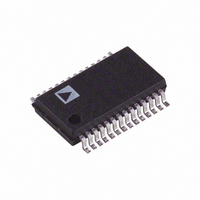
AD9822JRSZ Analog Devices Inc, AD9822JRSZ Datasheet

AD9822JRSZ
Specifications of AD9822JRSZ
Available stocks
Related parts for AD9822JRSZ
AD9822JRSZ Summary of contents
Page 1
FEATURES 14-bit 15 MSPS ADC No missing codes guaranteed 3-channel operation MSPS 1-channel operation up to 12.5 MSPS Correlated double sampling 1–6× programmable gain ±350 mV programmable offset Input clamp circuitry Internal voltage reference Multiplexed byte-wide output ...
Page 2
AD9822 TABLE OF CONTENTS Specifications..................................................................................... 3 Analog Specifications................................................................... 3 Digital Specifications ................................................................... 4 Timing Specifications .................................................................. 5 Absolute Maximum Ratings............................................................ 6 Thermal Characteristics .............................................................. 6 ESD Caution.................................................................................. 6 Pin Configuration and Function Descriptions............................. 7 Terminology ...................................................................................... 8 Functional Description .................................................................. ...
Page 3
SPECIFICATIONS ANALOG SPECIFICATIONS AVDD = 5 V, DRVDD = 5 V, CDS mode, f MIN MAX Table 1. Parameter MAXIMUM CONVERSION RATE 3-Channel Mode with CDS 1-Channel Mode with CDS ACCURACY (ENTIRE SIGNAL PATH) ADC Resolution ...
Page 4
AD9822 Parameter POWER DISSIPATION 3-Channel Mode 3-Channel Mode @ 6 MHz 1-Channel Mode 1-Channel Mode @ 6 MHz 1 Linear input signal range is from when the CCD’s reference level is clamped ...
Page 5
TIMING SPECIFICATIONS AVDD = 5 V, DRVDD = 5 V. MIN MAX Table 3. Parameter CLOCK PARAMETERS 3-Channel Pixel Rate 1-Channel Pixel Rate ADCCLK Pulse Width CDSCLK1 Pulse Width CDSCLK2 Pulse Width CDSCLK1 Falling to CDSCLK2 ...
Page 6
AD9822 ABSOLUTE MAXIMUM RATINGS Table 4. With Respect Parameter To Min VIN, CAPT, CAPB AVSS −0.3 Digital Inputs AVSS −0.3 AVDD AVSS −0.5 DRVDD DRVSS −0.5 AVSS DRVSS −0.3 Digital Outputs DRVSS −0.3 Junction Temperature Storage Temperature −65 Lead Temperature ...
Page 7
PIN CONFIGURATION AND FUNCTION DESCRIPTIONS Table 5. Pin Function Descriptions Pin No. Mnemonic Type 1 CDSCLK1 DI 2 CDSCLK2 DI 3 ADCCLK DI 4 OEB DI 5 DRVDD P 6 DRVSS (MSB ...
Page 8
AD9822 TERMINOLOGY Integral Nonlinearity (INL) Integral nonlinearity error refers to the deviation of each individual code from a line drawn from zero scale through positive full scale. The point used as zero scale occurs ½ LSB before the first code ...
Page 9
ANALOG t INPUTS AD PIXEL N ( CDSCLK1 t C1C2 CDSCLK2 t ADCLK t ADC2 ADCCLK t ADCLK OUTPUT DATA R (N– (N– (N– (N– (N– 2) ...
Page 10
AD9822 ANALOG INPUTS CDSCLK2 t ADCLK ADCCLK t ADCLK OUTPUT DATA R (N– (N– (N– (N– (N– (N– (N– (N– (N– (N– ...
Page 11
ADCCLK t OD OUTPUT HIGH BYTE LOW BYTE DATA DB13–DB6 DB5–DB0 <D7:D0> PIXEL N PIXEL N OEB SDATA R/ SCLK t LS SLOAD SDATA R/ SCLK t LS SLOAD ...
Page 12
AD9822 FUNCTIONAL DESCRIPTION The AD9822 can be operated in four different modes: 3-channel CDS mode, 3-channel SHA mode, 1-channel CDS mode, and 1-channel SHA mode. Each mode is selected by programming the configuration register through the serial interface. For more ...
Page 13
INTERNAL REGISTER DESCRIPTIONS Table 6. Internal Register Map Register Name Address Configuration MUX Red PGA Green PGA Blue PGA Red Offset 1 ...
Page 14
AD9822 PGA Gain Registers There are three PGA registers for individually programming the gain in the red, green, and blue channels. Bits D8, D7, and D6 in each register must be set low, and Bits D5 through D0 control the ...
Page 15
CIRCUIT OPERATION ANALOG INPUTS—CDS MODE Figure 10 shows the analog input configuration for the CDS mode of operation. Figure 11 shows the internal timing for the sampling switches. The CCD reference level is sampled when CDSCLK1 transitions from high to ...
Page 16
AD9822 ANALOG INPUTS—SHA MODE Figure 12 shows the analog input configuration for the SHA mode of operation. Figure 13 shows the internal timing for the sampling switches. The input signal is sampled when CDSCLK2 transitions from high to low, opening ...
Page 17
APPLICATIONS CIRCUIT AND LAYOUT RECOMMENDATIONS Figure 16 shows the recommended circuit configuration for 3-channel CDS mode operation. The recommended input coupling capacitor value is 0.1 µF (see the Circuit Operation section). A single ground plane is recommended for the AD9822. ...
Page 18
... Model Temperature Range AD9822JR 0°C to 70°C AD9822JRRL 0°C to 70°C AD9822JRS 0°C to 70°C AD9822JRSRL 0°C to 70°C 1 AD9822JRSZ 0°C to 70°C 1 AD9822JRSZRL 0°C to 70° Pb-free part. 18.10 (0.7126) 17.70 (0.6969 7.60 (0.2992) 7.40 (0.2913 2.65 (0.1043) 2.35 (0.0925) 1 ...
Page 19
NOTES Rev Page AD9822 ...
Page 20
AD9822 NOTES © 2005 Analog Devices, Inc. All rights reserved. Trademarks and registered trademarks are the property of their respective owners. C00623–0–2/05(B) Rev Page ...


