AD598AD Analog Devices Inc, AD598AD Datasheet

IC LVDT SIGNAL COND 20-CDIP

AD598AD

Manufacturer Part Number
AD598AD
Description
IC LVDT SIGNAL COND 20-CDIP
Manufacturer
Analog Devices Inc
Type
Signal Conditionerr
Datasheets

Specifications of AD598AD

Rohs Status
RoHS non-compliant
Input Type
Voltage
Output Type
Voltage
Interface
LVDT
Current - Supply
15mA
Mounting Type
Through Hole
Package / Case
20-CDIP (0.300", 7.62mm)
Bandwidth
20kHz
Supply Voltage Min
13V
Supply Voltage Max
36V
Digital Ic Case Style
DIP
No. Of Pins
20
Operating Temperature Range
-40°C To +85°C
Temperature Coefficient
250ppm/°C
Application
Proving ring-weigh scale, synchronous opeation of multiple LVDTS
Converter Type
voltage to Frequency
Current, Output
6 mA (Min.)
Impedance, Input
200 Kiloohms (Typ.)
Package Type
Ceramic DIP
Temperature, Operating, Maximum
85 °C
Temperature, Operating, Minimum
-40 °C
Voltage, Operating
36 V (Max.)
Lead Free Status / RoHS Status
Contains lead / RoHS non-compliant

Available stocks

Company
Part Number
Manufacturer
Quantity
Price
Part Number:
AD598AD
Manufacturer:
AD
Quantity:
3 270
Part Number:
AD598AD
Manufacturer:
AD
Quantity:
3 270
Part Number:
AD598AD
Manufacturer:
ADI
Quantity:
529
Part Number:
AD598AD
Manufacturer:
AD
Quantity:
1 520
Part Number:
AD598AD
Manufacturer:
ADI/亚德诺
Quantity:
20 000
a
FEATURES
Single Chip Solution, Contains Internal Oscillator and
No Adjustments Required
Insensitive to Transducer Null Voltage
Insensitive to Primary to Secondary Phase Shifts
DC Output Proportional to Position
20 Hz to 20 kHz Frequency Range
Single or Dual Supply Operation
Unipolar or Bipolar Output
Will Operate a Remote LVDT at Up to 300 Feet
Position Output Can Drive Up to 1000 Feet of Cable
Will Also Interface to an RVDT
Outstanding Performance
PRODUCT DESCRIPTION
The AD598 is a complete, monolithic Linear Variable Differen-
tial Transformer (LVDT) signal conditioning subsystem. It is
used in conjunction with LVDTs to convert transducer mechan-
ical position to a unipolar or bipolar dc voltage with a high
degree of accuracy and repeatability. All circuit functions are
included on the chip. With the addition of a few external passive
components to set frequency and gain, the AD598 converts the
raw LVDT secondary output to a scaled dc signal. The device
can also be used with RVDT transducers.
The AD598 contains a low distortion sine wave oscillator to
drive the LVDT primary. The LVDT secondary output consists
of two sine waves that drive the AD598 directly. The AD598
operates upon the two signals, dividing their difference by their
sum, producing a scaled unipolar or bipolar dc output.
The AD598 uses a unique ratiometric architecture (patent pend-
ing) to eliminate several of the disadvantages associated with
traditional approaches to LVDT interfacing. The benefits of this
new circuit are: no adjustments are necessary, transformer null
voltage and primary to secondary phase shift does not affect sys-
tem accuracy, temperature stability is improved, and transducer
interchangeability is improved.
The AD598 is available in two performance grades:
Grade
AD598JR 0 C to +70 C
AD598AD –40 C to +85 C
It is also available processed to MIL-STD-883B, for the military
range of –55 C to +125 C.
REV. A
Information furnished by Analog Devices is believed to be accurate and
reliable. However, no responsibility is assumed by Analog Devices for its
use, nor for any infringements of patents or other rights of third parties
which may result from its use. No license is granted by implication or
otherwise under any patent or patent rights of Analog Devices.
Voltage Reference
Linearity: 0.05% of FS max
Output Voltage:
Gain Drift: 50 ppm/ C of FS max
Offset Drift: 50 ppm/ C of FS max
Temperature Range Package
11 V min
20-Pin Small Outline (SOIC)
20-Pin Ceramic DIP
PRODUCT HIGHLIGHTS
1. The AD598 offers a monolithic solution to LVDT and
2. The AD598 can be used with many different types of
3. The 20 Hz to 20 kHz LVDT excitation frequency is deter-
4. The AD598 uses a ratiometric decoding scheme such that
5. Multiple LVDTs can be driven by a single AD598, either in
6. The AD598 may be used in telemetry applications or in hos-
7. The AD598 may be used as a loop integrator in the design of
One Technology Way, P.O. Box 9106, Norwood, MA 02062-9106, U.S.A.
Tel: 617/329-4700
RVDT signal conditioning problems; few extra passive com-
ponents are required to complete the conversion from me-
chanical position to dc voltage and no adjustments are
required.
LVDTs because the circuit accommodates a wide range of
input and output voltages and frequencies; the AD598 can
drive an LVDT primary with up to 24 V rms and accept sec-
ondary input levels as low as 100 mV rms.
mined by a single external capacitor. The AD598 input sig-
nal need not be synchronous with the LVDT primary drive.
This means that an external primary excitation, such as the
400 Hz power mains in aircraft, can be used.
primary to secondary phase shifts and transducer null voltage
have absolutely no effect on overall circuit performance.
series or parallel as long as power dissipation limits are not
exceeded. The excitation output is thermally protected.
tile environments where the interface electronics may be re-
mote from the LVDT. The AD598 can drive an LVDT at
the end of 300 feet of cable, since the circuit is not affected
by phase shifts or absolute signal magnitudes. The position
output can drive as much as 1000 feet of cable.
simple electromechanical servo loops.
LVDT
FUNCTIONAL BLOCK DIAGRAM
V
V
EXCITATION (CARRIER)
A
B
17
10
11
A–B
A+B
OSC
FILTER
AMP
Conditioner
LVDT Signal
3
AD598
AMP
2
AD598
Fax: 617/326-8703
16
V
OUT

Related parts for AD598AD

AD598AD Summary of contents

Page 1

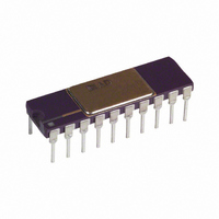
... The AD598 is available in two performance grades: Grade Temperature Range Package AD598JR +70 C 20-Pin Small Outline (SOIC) AD598AD – +85 C 20-Pin Ceramic DIP It is also available processed to MIL-STD-883B, for the military range of – +125 C. REV. A Information furnished by Analog Devices is believed to be accurate and reliable ...

Page 2

... V rms 2.1 1.2 2.1 V rms 4.1 2.6 4.1 V rms rms 600 ppm rms 12 mA rms 60 mA 100 30 100 mV 20k 20 20k Hz 200 ppm/ C –50 dB 3.5 0.1 3.5 V rms 200 kHz 17 +70 C –40 +85 C AD598AD REV. A ...

Page 3

... Storage Temperature Range R Package . . . . . . . . . . . . . . . . . . . . . . . . . – +150 C D Package . . . . . . . . . . . . . . . . . . . . . . . . . – +150 C Operating Temperature Range AD598JR . . . . . . . . . . . . . . . . . . . . . . . . . . . . +70 C AD598AD . . . . . . . . . . . . . . . . . . . . . . . . . . – +85 C Lead Temperature Range (Soldering 60 sec +300 C Power Dissipation 1.2 W Derates Above + mW/ C REV 1.65% of full scale. Note that 1000 ppm of full scale equals 0.1% of full scale. ...

Page 4

AD598–Typical Characteristics 40 OFFSET PSRR 12–15V 0 OFFSET PSRR 15–18V –40 GAIN PSRR 12–15V –80 –120 GAIN PSRR 15–18V –160 –200 –240 –60 – TEMPERATURE – C Figure 1. Gain and Offset PSRR vs. Temperature 5 0 ...

Page 5

This technique uses the pri- mary excitation voltage as a phase reference to determine the polarity of the output voltage. There are a number of problems associated with this technique such as (1) producing a ...

Page 6

AD598 DESIGN PROCEDURE DUAL SUPPLY OPERATION Figure 7 shows the connection method with dual 15 volt power supplies and a Schaevitz E100 LVDT. This design procedure can be used to select component values for other LVDTs as well. The procedure ...

Page 7

C2, C3 and C4 are a function of the desired bandwidth of the AD598 position measurement subsystem. They should be nominally equal values. – Farad Hz/f If the desired system bandwidth is ...

Page 8

AD598 13. Load current through R returns to the junction of R5 and L R6, and flows back Under maximum load condi- PS tions, make sure the voltage drop across R5 is met as defined in Step ...

Page 9

Figure 15. Gain and Phase Characteristics vs. Frequency (0 kHz–10 kHz) 1000 100 10 1 0.1 0.01 0.1 C2, C3, C4 – F Figure 16. Output Voltage Ripple vs. Filter Capacitance REV. A 1000 100 ...

Page 10

AD598–Applications PROVING RING-WEIGH SCALE Figure 20 shows an elastic member (steel proving ring) com- bined with an LVDT to provide a means of measuring very small loads. Figure 19 shows the electrical circuit details. The advantage of using a Proving ...

Page 11

MASTER – – OFFSET 1 19 EXC 1 OFFSET EXC LEV 1 SIG REF 82. LEV 2 SIG OUT 0.015 FEEDBACK ...

Page 12

AD598 The V/F converter is currently set up for unipolar operation. The AD652 data sheet explains how to set up for bipolar opera- tion. Note that when the LVDT core is centered, the output fre- quency is zero. When the ...

Page 13

OUTPUT MECHANICAL POSITION SCHAEVITZ E 100 LVDT 0.015 F 0.1 F INPUT MECHANICAL POSITION SCHAEVITZ E 100 LVDT 0.015 F 0 LVDT 1 SCHAEVITZ E 100 C D LVDT 2 SCHAEVITZ E 100 REV. A MASS ON ...

Page 14

AD598 PRECISION DIFFERENTIAL GAGING The circuit shown in Figure 26 is functionally similar to the dif- ferential gaging circuit shown in Figure 25. In contrast to Figure 25, it provides a means of independently adjusting the scale fac- tor of ...

Page 15

OPERATION WITH A HALF-BRIDGE TRANSDUCER Although the AD598 is not intended for use with a half-bridge type transducer, it may be made to function with degraded performance. A half-bridge type transducer is a popular transducer. It works in a similar ...

Page 16

AD598 OUTLINE DIMENSIONS Dimensions shown in inches and (mm). 20-Pin Sized Brazed Ceramic DIP 20-Lead Wide Body Plastic SOIC (R) Package –16– REV. A ...

Related keywords