AD598AD Analog Devices Inc, AD598AD Datasheet - Page 2
AD598AD
Manufacturer Part Number
AD598AD
Description
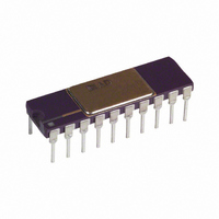
IC LVDT SIGNAL COND 20-CDIP
Manufacturer
Analog Devices Inc
Type
Signal Conditionerr
Specifications of AD598AD
Rohs Status
RoHS non-compliant
Input Type
Voltage
Output Type
Voltage
Interface
LVDT
Current - Supply
15mA
Mounting Type
Through Hole
Package / Case
20-CDIP (0.300", 7.62mm)
Bandwidth
20kHz
Supply Voltage Min
13V
Supply Voltage Max
36V
Digital Ic Case Style
DIP
No. Of Pins
20
Operating Temperature Range
-40°C To +85°C
Temperature Coefficient
250ppm/°C
Application
Proving ring-weigh scale, synchronous opeation of multiple LVDTS
Converter Type
voltage to Frequency
Current, Output
6 mA (Min.)
Impedance, Input
200 Kiloohms (Typ.)
Package Type
Ceramic DIP
Temperature, Operating, Maximum
85 °C
Temperature, Operating, Minimum
-40 °C
Voltage, Operating
36 V (Max.)
Lead Free Status / RoHS Status
Contains lead / RoHS non-compliant
Available stocks
Company
Part Number
Manufacturer
Quantity
Price

Part Number:
AD598AD
Manufacturer:
ADI/亚德诺
Quantity:
20 000


AD598–SPECIFICATIONS
Parameter
TRANSFER FUNCTION
OVERALL ERROR
SIGNAL OUTPUT CHARACTERISTICS
EXCITATION OUTPUT CHARACTERISTICS (@ 2.5 kHz)
SIGNAL INPUT CHARACTERISTICS
POWER SUPPLY REQUIREMENTS
TEMPERATURE RANGE
PACKAGE OPTION
T
Output Voltage Range (T
Output Current (T
Short Circuit Current
Nonlinearity
Gain Error
Gain Drift
Offset
Offset Drift
Excitation Voltage Rejection
Power Supply Rejection ( 12 V to 18 V)
Common-Mode Rejection ( 3 V)
Excitation Voltage Range
Excitation Voltage
Excitation Voltage TC
Output Current
Short Circuit Current
DC Offset Voltage (Differential, R1 = 12.7 k )
Frequency
Frequency TC, (R1 = 12.7 k )
Total Harmonic Distortion
Signal Voltage
Input Impedance
Input Bias Current (AIN and BIN)
Signal Reference Bias Current
Excitation Frequency
Operating Range
Dual Supply Operation ( 10 V Output)
Single Supply Operation
Current (No Load at Signal and Excitation Outputs)
JR (SOIC)
AD (DIP)
SOIC (R-20)
Side Brazed DIP (D-20)
MIN
PSRR Gain (T
PSRR Offset (T
CMRR Gain (T
CMRR Offset (T
Output Ripple
(R1 = Open)
(R1 = 12.7 k )
(R1 = 487 )
T
T
0 to +10 V Output
0 to –10 V Output
T
MIN
MIN
MIN
to T
5
to T
to T
to T
MAX
4
3
MAX
MAX
MAX
(T
8
8
MIN
7
MIN
8
2
MIN
MIN
MIN
MIN
to T
to T
to T
to T
9
to T
to T
1
MAX
MIN
MAX
MAX
MAX
MAX
MAX
6
)
)
to T
)
)
)
)
MAX
)
(typical @ +25 C and 15 V dc, C1 = 0.015 F, R2 = 80 k , R
unless otherwise noted. See Figure 7.)
Min
8
300
100
100
100
2.1
1.2
2.6
14
30
12
20
0.1
0
13
17.5
17.5
0
–2–
13
11
AD598JR
AD598J
Typ
V
0.6
20
75
0.4
20
0.3
7
100
100
15
25
6
4
600
60
30
200
–50
200
1
2
12
OUT
Max
2.35
24
2.1
4.1
20
20k
3.5
5
10
20
36
15
16
+70
V
V
A
A
500
1
100
1
200
100
–V
V
B
B
20
Min
6
400
200
200
200
2.1
1.2
2.6
14
30
12
0.1
0
13
17.5
17.5
–40
13
11
AD598AD
500 A R2
AD598A
Typ
0.6
20
75
0.4
20
0.3
7
100
100
15
25
6
4
600
60
30
200
–50
200
1
2
12
20k
Max
1.65
24
2.1
4.1
20
3.5
5
10
20
36
15
18
+85
500
1
50
1
50
100
L
= 2 k ,
Unit
V
% of FS
V
mA
mA
ppm of FS
% of FS
ppm/ C of FS
% of FS
ppm/ C of FS
ppm/dB
ppm/V
ppm/V
ppm/V
ppm/V
mV rms
V rms
V rms
V rms
V rms
ppm/ C
mA rms
mA rms
mA
mV
Hz
ppm/ C
dB
V rms
k
kHz
V
V
V
V
mA
mA
C
C
A
A
REV. A
Related parts for AD598AD
Image
Part Number
Description
Manufacturer
Datasheet
Request
R

Part Number:
Description:
±1.7g Dual-Axis IMEMS Accelerometer Evaluation Board
Manufacturer:
Analog Devices Inc
Datasheet:

Part Number:
Description:
Inertial Sensor Evaluation System
Manufacturer:
Analog Devices Inc
Datasheet:
Part Number:
Description:
Manufacturer:
Analog Devices Inc
Datasheet:
Part Number:
Description:
Manufacturer:
Analog Devices Inc
Datasheet:
Part Number:
Description:
Manufacturer:
Analog Devices Inc
Datasheet:
Part Number:
Description:
Manufacturer:
Analog Devices Inc
Datasheet:
Part Number:
Description:
Manufacturer:
Analog Devices Inc
Datasheet:
Part Number:
Description:
Manufacturer:
Analog Devices Inc
Datasheet:
Part Number:
Description:
Manufacturer:
Analog Devices Inc
Datasheet:
Part Number:
Description:
Manufacturer:
Analog Devices Inc
Datasheet:
Part Number:
Description:
Manufacturer:
Analog Devices Inc
Datasheet:
Part Number:
Description:
Manufacturer:
Analog Devices Inc
Datasheet:
Part Number:
Description:
Manufacturer:
Analog Devices Inc
Datasheet: