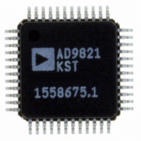
AD9821KSTZ Analog Devices Inc, AD9821KSTZ Datasheet - Page 12

AD9821KSTZ
Manufacturer Part Number
AD9821KSTZ
Description
IC IMAGE SGNL PROC 12BIT 48-LQFP
Manufacturer
Analog Devices Inc
Type
Image Sensorr
Datasheet
1.AD9821KST.pdf
(16 pages)
Specifications of AD9821KSTZ
Input Type
Logic
Output Type
Logic
Interface
3-Wire Serial
Mounting Type
Surface Mount
Package / Case
48-LQFP
Analog Front End Type
CCD
Analog Front End Category
Video
Interface Type
Serial (3-Wire)
Sample Rate
40MSPS
Input Voltage Range
0.5V
Operating Supply Voltage (min)
2.7V
Operating Supply Voltage (typ)
3.3V
Operating Supply Voltage (max)
3.6V
Resolution
12b
Number Of Adc's
1
Power Supply Type
Analog/Digital
Operating Temp Range
-20C to 85C
Operating Temperature Classification
Commercial
Mounting
Surface Mount
Pin Count
48
Package Type
LQFP
Number Of Channels
1
Lead Free Status / RoHS Status
Lead free / RoHS Compliant
Current - Supply
-
Lead Free Status / RoHS Status
Compliant, Lead free / RoHS Compliant
Available stocks
Company
Part Number
Manufacturer
Quantity
Price
AD9821
Variable Gain Amplifier
The VGA stage provides a gain range of 0 dB to 36 dB, program-
mable with 10-bit resolution through the serial digital interface. A
minimum gain of 6 dB is needed to match a 1 V input signal with
the ADC full-scale range of 2 V. When compared to 1 V full-scale
systems, the equivalent gain range is –6 dB to +30 dB.
The VGA gain curve follows a “linear-in-dB” characteristic.
The exact VGA gain can be calculated for any Gain Register
value by using the equation:
where the code range is 0 to 1023.
Optical Black Clamp
The optical black clamp loop is used to remove residual offsets
in the signal chain, and to track low frequency variations in the
CCD’s black level. During the optical black (shielded) pixel
interval on each line, the ADC output is compared with a fixed
black level reference selected by the user in the Clamp Level
Register. Any value between 0 LSB and 255 LSB may be
36
30
24
18
12
6
0
0
127
Figure 11. VGA Gain Curve
Gain dB
255
(
VGA GAIN REGISTER CODE
383
) ( .
=
0 0351
511
639
×
Code
767
)
895
1023
–12–
programmed using the 8-bit Clamp Level Register. The resulting
error signal is filtered to reduce noise, and the correction value is
applied to the ADC input through a D/A converter. Normally, the
optical black clamp loop is turned on once per horizontal line, but
this loop can be updated more slowly to suit a particular
application. If external digital clamping is used during the post-
processing, the AD9821 optical black clamping may be disabled
using Bit D5 in the Operation Register (see Internal Register
Map and Serial Interface Timing section). When the loop is
disabled, the Clamp Level Register may still be used to provide
programmable offset adjustment.
Horizontal timing is shown in Figure 9. The CLPOB pulse
should be placed during the CCD’s optical black pixels. It is
recommended that the CLPOB pulse duration be at least 20
pixels wide. Shorter pulsewidths may be used, but the ability to
track low frequency variations in the black level will be reduced.
As discussed in the Differential Input SHA section, the CLPOB
loop is capable of correcting for an offset difference between the
VIN+ and VIN– inputs. Because the clamp is located after the
VGA gain stage, the clamp will be most limited when the VGA
gain is at its maximum value. Under these conditions, the OB
clamp loop correction range is restricted to ± 30 mV offset
between the VIN+ and VIN– inputs. At minimum VGA gain,
the offset correction range increases to ± 250 mV of offset. If the
OB clamp loop’s correction range is exceeded, then the black
level at the output of the AD9821 will increase and further
correction will be necessary. As mentioned previously, it is also
possible to disable the AD9821’s OB clamp loop.
A/D Converter (ADC)
The AD9821 uses high performance ADC architecture, opti-
mized for high speed and low power. Differential nonlinearity
(DNL) performance is typically better than 0.5 LSB, as shown in
TPC 2. Instead of the 1 V full-scale range used by the earlier
AD9801 and AD9803 products from Analog Devices, the
AD9821’s ADC uses a 2 V input range. Better noise performance
results from using a larger ADC full-scale range (see TPC 3).
REV. 0


