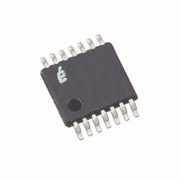
X96012V14I Intersil, X96012V14I Datasheet - Page 6

X96012V14I
Manufacturer Part Number
X96012V14I
Description
IC CNTRLR UNIV MEM/DAC 14-TSSOP
Manufacturer
Intersil
Type
Controllerr
Datasheet
1.X96012V14IZT1.pdf
(23 pages)
Specifications of X96012V14I
Input Type
*
Output Type
*
Interface
2-Wire Serial
Current - Supply
*
Mounting Type
Surface Mount
Package / Case
14-TSSOP
Lead Free Status / RoHS Status
Contains lead / RoHS non-compliant
Available stocks
Company
Part Number
Manufacturer
Quantity
Price
Company:
Part Number:
X96012V14I
Manufacturer:
Intersil
Quantity:
1 050
Part Number:
X96012V14IZ
Manufacturer:
INTERSIL
Quantity:
20 000
2-Wire Interface Test Conditions
A/D Converter Characteristics
NOTES:
14. LSB” is defined as V(VRef)/255, “Full-Scale” is defined as V(VRef).
15. Offset
2-Wire Interface AC Characteristics
Input Pulse Levels
Input Rise and Fall Times, between 10% and 90%
Input and Output Timing Threshold Level
External Load at Pin SDA
f
t
t
t
t
t
t
t
t
t
t
t
t
t
t
t
Cb (Note 2)
SCL
IN
AA
BUF
LOW
HIGH
SU:STA
HD:STA
SU:DAT
HD:DAT
SU:STO
DH
R
F
SU:WP
HD:WP
(Note 2)
(Note 2)
SYMBOL
(Note 2)
deviation between the measured first transition point and the ideal point. FSError
curve occurs at
after subtracting the Offset from the measured curve. DNL
transitions for successive A/D code outputs expressed in LSBs. The measured transfer curve is adjusted for Offset and Full-scale errors before
calculating DNL. INL
also defined as the sum of the DNL errors starting from code 00h to the code where the INL measurement is desired. The measured transfer
curve is adjusted for Offset and Full scale errors before calculating INL.
(Note 2)
SYMBOL
(Note 2)
(Note 2)
(Note 2)
ADC
: For an ideal converter, the first transition of its transfer curve occurs at
[
SCL Clock Frequency
Pulse width Suppression Time at Inputs
SCL Low to SDA Data Out Valid
Time the Bus Free Before Start of New
Transmission
Clock Low Time
Clock High Time
Start Condition Set-up Time
Start Condition Hold Time
Data In Set-up Time
Data In Hold Time
Stop Condition Set-up Time
Data Output Hold Time
SDA and SCL Rise Time
SDA and SCL Fall Time
WP Set-up Time
WP Hold Time
Capacitive Load for Each Bus Line
254.5 x V(VRef)
ADC
PARAMETER
255
: The deviation of the measured transfer function of an A/D converter from the ideal transfer function. The INL error is
6
PARAMETER
]
. Full-Scale Error is the amount of deviation between the measured last transition point and the ideal point,
(See “Electrical Specifications” table starting on page 3 for standard conditions).
ADC
TEST CONDITIONS
See “2-Wire Interface Test
Conditions” on page 6
See Figures 1, 2, 3.
: DNL is defined as the difference between the ideal and the measured code
X96012
TEST CONDITIONS
ADC
[
0.5 x V(VRef)
: For an ideal converter, the last transition of its transfer
255
10% to 90% of V
10ns
1.4V
2.3kΩ to V
(Note 3)
MIN
20 +0.1Cb
20 +0.1Cb
]
(Note 18)
(Note 16)
(Note 16)
(Note 3)
1300
above zero. Offset error is the amount of
MIN
600
600
100
600
600
600
1.3
0.6
CC
50
1
0
and 100pF to V
CC
TYP
TYP
(Note 18)
(Note 18)
(Note 3)
SS
(Note 3)
MAX
1200
1200
400
900
300
300
400
50
MAX
February 20, 2008
UNITS
kHz
UNIT
FN8216.3
pF
ns
ns
ns
µs
µs
ns
ns
ns
µs
ns
ns
ns
ns
ns
ns


