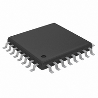
MAX3693ECJ+ Maxim Integrated Products, MAX3693ECJ+ Datasheet - Page 6

MAX3693ECJ+
Manufacturer Part Number
MAX3693ECJ+
Description
IC 4:1 SERIALIZER 622MBPS 32TQFP
Manufacturer
Maxim Integrated Products
Datasheet
1.MAX3693ECJ.pdf
(8 pages)
Specifications of MAX3693ECJ+
Function
Serializer
Data Rate
622Mbps
Input Type
LVDS
Output Type
PECL
Number Of Inputs
4
Number Of Outputs
1
Voltage - Supply
3 V ~ 3.6 V
Operating Temperature
-40°C ~ 85°C
Mounting Type
Surface Mount
Package / Case
32-LQFP
Lead Free Status / RoHS Status
Lead free / RoHS Compliant
The MAX3693 features LVDS inputs and outputs for
interfacing with high-speed digital circuitry. The LVDS
standard is based on the IEEE 1596.3 LVDS specifi-
cation. This technology uses 250mV to 400mV differ-
ential low-voltage swings to achieve fast transition
times, minimized power dissipation, and noise immu-
nity.
For proper operation, the parallel-clock LVDS outputs
(PCLKO+, PCLKO-) require 100Ω differential DC termi-
+3.3V, 622Mbps, SDH/SONET 4:1 Serializer
with Clock Synthesis and LVDS Inputs
Figure 2. Timing Diagram
6
_______________________________________________________________________________________
Low-Voltage Differential-Signal (LVDS)
PCLKO
PCLKI
PD_
SD
NOTE: SIGNALS SHOWN ARE DIFFERENTIAL. FOR EXAMPLE, PCLKO = (PCLKO+) - (PCLKO-).
*PD3 = D3; PD2 = D2; PD1 = D1; PD0 = D0.
VALID PARALLEL DATA*
Inputs and Outputs
t
SU
t
SKEW
t
H
nation between the inverting and noninverting outputs.
Do not terminate these outputs to ground.
The parallel data and parallel clock LVDS inputs (PD_+,
PD_-, PCLKI+, PCLKI-, RCLK+, RCLK-) are internally
terminated with 100Ω differential input resistance, and
therefore do not require external termination.
The serial-data PECL outputs (SD+, SD-) require 50Ω
DC termination to (V
Output Termination section).
D3
CC
D2
- 2V) (see the Alternative PECL-
D1
D0
PECL Outputs


