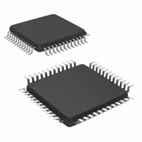
DS90C241IVSX/NOPB National Semiconductor, DS90C241IVSX/NOPB Datasheet

DS90C241IVSX/NOPB
Specifications of DS90C241IVSX/NOPB
Available stocks
Related parts for DS90C241IVSX/NOPB
DS90C241IVSX/NOPB Summary of contents
Page 1
... User defined Pre-Emphasis driving ability through external resistor on LVDS outputs and capable to drive meters shielded twisted-pair cable Block Diagram TRI-STATE ® registered trademark of National Semiconductor Corporation. © 2009 National Semiconductor Corporation DS90C241/DS90C124 ■ User selectable clock edge for parallel data on both Transmitter and Receiver ■ ...
Page 2
... Absolute Maximum Ratings If Military/Aerospace specified devices are required, please contact the National Semiconductor Sales Office/ Distributors for availability and specifications. Supply Voltage ( LVCMOS/LVTTL Input Voltage LVCMOS/LVTTL Output Voltage LVDS Receiver Input Voltage LVDS Driver Output Voltage LVDS Output Short Circuit Duration ...
Page 3
Symbol Parameter V Output Differential Voltage OD (D )–(D ) OUT+ OUT− ΔV Output Differential Voltage OD Unbalance V Offset Voltage OS ΔV Offset Voltage Unbalance OS I Output Short Circuit Current OS I TRI-STATE Output Current OZ SER/DES SUPPLY ...
Page 4
Serializer Timing Requirements for TCLK Over recommended operating supply and temperature ranges unless otherwise specified. Symbol Parameter t Transmit Clock Period TCP t Transmit Clock High Time TCIH t Transmit Clock Low Time TCIL t TCLK Input Transition Time CLKT ...
Page 5
Symbol Parameter t ROUT (23:16) Setup Data to ROS RCLK (Group 3) t ROUT (23:16) Hold Data to ROH RCLK (Group 3) t HIGH to TRI-STATE Delay HZR t LOW to TRI-STATE Delay LZR t TRI-STATE to HIGH Delay ZHR ...
Page 6
AC Timing Diagrams and Test Circuits FIGURE 3. Serializer LVDS Output Load and Transition Times www.national.com FIGURE 1. Serializer Input Checker-board Pattern FIGURE 2. Deserializer Output Checker-board Pattern FIGURE 4. Serializer Input Clock Transition Times 6 20171902 20171903 20171904 20171906 ...
Page 7
FIGURE 5. Serializer Setup/Hold Times FIGURE 6. Serializer TRI-STATE Test Circuit and Delay 7 20171907 20171908 www.national.com ...
Page 8
FIGURE 7. Serializer PLL Lock Time, and TPWDNB TRI-STATE Delays FIGURE 9. Transmitter Output Eye Opening (TxOUT_E_O) www.national.com FIGURE 8. Serializer Delay 8 20171909 20171910 20171915 ...
Page 9
VOD = (D ) – OUT+ OUT - Differential output signal is shown – (D OUT+ FIGURE 11. Deserializer LVCMOS/LVTTL Output Load and Transition Times ), device in Data Transfer mode. OUT - FIGURE 10. ...
Page 10
Note: C includes instrumentation and fixture capacitance within ROUT[23:0] L FIGURE 13. Deserializer TRI-STATE Test Circuit and Timing FIGURE 14. Deserializer PLL Lock Times and RPWDNB TRI-STATE Delay www.national.com 20171913 10 20171914 ...
Page 11
RxIN_TOL_L is the ideal noise margin on the left of the figure, with respect to ideal. RxIN_TOL_R is the ideal noise margin on the right of the figure, with respect to ideal. FIGURE 16. Receiver Input Tolerance (RxIN_TOL) and Sampling ...
Page 12
DS90C241 Serializer Pin Descriptions Pin # Pin Name I/O LVCMOS PARALLEL INTERFACE PINS 4-1, DIN[23:0] LVCMOS_I 48-44, 41-32, 29-25 10 TCLK LVCMOS_I CONTROL AND CONFIGURATION PINS 9 TPWDNB LVCMOS_I 18 DEN LVCMOS_I 23 PRE LVCMOS_I 11 TRFB LVCMOS_I 12 VODSEL ...
Page 13
Pin # Pin Name I/O 43 VSSIT GND 24 VSS GND DS90C241 Pin Diagram Digital Ground, Tx Input Ground ESD Ground Serializer - DS90C241 TOP VIEW 13 Description 20171919 www.national.com ...
Page 14
DS90C124 Deserializer Pin Descriptions Pin # Pin Name I/O LVCMOS PARALLEL INTERFACE PINS 25-28, ROUT[7:0] LVCMOS_O 31-34 13-16, ROUT[15:8] LVCMOS_O 21-24 3-6, ROUT[23:16] LVCMOS_O 9-12 18 RCLK LVCMOS_O CONTROL AND CONFIGURATION PINS 43 RRFB LVCMOS_I 48 REN LVCMOS_I 1 RPWDNB ...
Page 15
DS90C124 Pin Diagram Deserializer - DS90C124 TOP VIEW 15 20171920 www.national.com ...
Page 16
Functional Description The DS90C241 Serializer and DS90C124 Deserializer chipset is an easy-to-use transmitter and receiver pair that sends 24-bits of parallel LVCMOS data over a single serial LVDS link from 120 Mbps to 840 Mbps throughput. The DS90C241 transforms a ...
Page 17
The Serializer enters powerdown when the TPWDNB pin is driven low. In power- down, the PLL stops and the outputs go into ...
Page 18
Applications Information USING THE DS90C241 AND DS90C124 The DS90C241/DS90C124 (SERDES) pair sends 24 bits of parallel LVCMOS data over a serial LVDS link up to 840 Mbps. Serialization of the input data is accomplished using an on-board PLL at the ...
Page 19
The tightly coupled lines will also radiate less. Termination of the LVDS interconnect is required. For point- to-point applications, termination should ...
Page 20
FIGURE 18. DS90C241 Tyical Application Connection 20 20171921 ...
Page 21
FIGURE 19. DS90C124 Tyical Application Connection 21 20171922 www.national.com ...
Page 22
FIGURE 20. Receiver Termination Option 2 FIGURE 21. Receiver Termination Option 3 22 20171923 20171924 ...
Page 23
Truth Tables TPWDNB (Pin 9) (Pin 18 RPWDNB REN (Pin 1) (Pin 48 TABLE 1. DS90C241 Serializer Truth Table DEN Tx PLL Status (Internal ...
Page 24
Physical Dimensions Ordering Information NSID DS90C241QVS 48 Lead TQFP style, 7.0 X 7.0 X 1.0 mm, 0.5 mm pitch DS90C241QVSX 48 Lead TQFP style, 7.0 X 7.0 X 1.0 mm, 0.5 mm pitch, 1000 std reel DS90C241IVS 48 Lead TQFP ...
Page 25
Notes 25 www.national.com ...
Page 26
... For more National Semiconductor product information and proven design tools, visit the following Web sites at: Products Amplifiers www.national.com/amplifiers Audio www.national.com/audio Clock and Timing www.national.com/timing Data Converters www.national.com/adc Interface www.national.com/interface LVDS www.national.com/lvds Power Management www.national.com/power Switching Regulators www.national.com/switchers LDOs www.national.com/ldo LED Lighting www ...


