DS10BR150TSD/NOPB National Semiconductor, DS10BR150TSD/NOPB Datasheet - Page 3
DS10BR150TSD/NOPB
Manufacturer Part Number
DS10BR150TSD/NOPB
Description
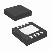
IC BUFFER/REPEATER LVDS 8-LLP
Manufacturer
National Semiconductor
Type
Bufferr
Datasheet
1.DS10BR150TSDNOPB.pdf
(12 pages)
Specifications of DS10BR150TSD/NOPB
Tx/rx Type
LVDS
Delay Time
380ps
Capacitance - Input
1.7pF
Voltage - Supply
3 V ~ 3.6 V
Current - Supply
21mA
Mounting Type
Surface Mount
Package / Case
8-LLP
Number Of Elements
1
Number Of Receivers
1
Number Of Drivers
1
Operating Supply Voltage (typ)
3.3V
Differential Input High Threshold Voltage
100mV
Diff. Input Low Threshold Volt
-100mV
Output Type
Repeater
Differential Output Voltage
450mV
Transmission Data Rate
1000Mbps
Propagation Delay Time
0.6ns
Power Dissipation
2.08W
Operating Temp Range
-40C to 85C
Operating Temperature Classification
Industrial
Mounting
Surface Mount
Pin Count
8
Data Rate
1 Gbps
Operating Supply Voltage
3.3 V
Maximum Power Dissipation
2080 mW
Maximum Operating Temperature
+ 85 C
Minimum Operating Temperature
- 40 C
Mounting Style
SMD/SMT
Supply Voltage (max)
3.6 V
Supply Voltage (min)
3 V
Supply Current
21mA
Supply Voltage Range
3V To 3.6V
Driver Case Style
LLP
No. Of Pins
8
Operating Temperature Range
-40°C To +85°C
Msl
MSL 3 - 168 Hours
Filter Terminals
SMD
Logic Type
Buffer
Rohs Compliant
Yes
Data Rate Max
1Gbps
For Use With
DS10BR150EVK - BOARD EVALUATION DS10BR150
Lead Free Status / RoHS Status
Lead free / RoHS Compliant
Other names
DS10BR150TSD
DS10BR150TSDTR
DS10BR150TSDTR
Available stocks
Company
Part Number
Manufacturer
Quantity
Price
Company:

Part Number:
DS10BR150TSD/NOPB
Manufacturer:
LT
Quantity:
300


LVDS OUTPUT DC SPECIFICATIONS (OUT+, OUT-)
V
ΔV
V
ΔV
I
C
R
LVDS INPUT DC SPECIFICATIONS (IN+, IN-)
V
V
V
V
I
C
R
SUPPLY CURRENT
I
Symbol
OS
IN
CCD
Supply Voltage (V
LVDS Input Voltage (IN+, IN−)
LVDS Differential Input Voltage ((IN+) - (IN−))
LVDS Output Voltage (OUT+, OUT−)
LVDS Differential Output Voltage ((OUT+) - (OUT−))
LVDS Output Short Circuit Current
Duration
Junction Temperature
Storage Temperature Range
Lead Temperature Range
Maximum Package Power Dissipation at 25°C
OD
OS
ID
TH
TL
CMR
OUT
OUT
IN
IN
Absolute Maximum Ratings
If Military/Aerospace specified devices are required,
please contact the National Semiconductor Sales Office/
Distributors for availability and specifications.
DC Electrical Characteristics
Over recommended operating supply and temperature ranges unless otherwise specified. (Notes 5, 6, 7)
OD
OS
Soldering (4 sec.)
SDA Package
Derate SDA Package
Differential Output Voltage
Change in Magnitude of V
Output States
Offset Voltage
Change in Magnitude of V
Output States
Output Short Circuit Current (Note 8)
Output Capacitance
Output Termination Resistor
Input Differential Voltage
Differential Input High Threshold
Differential Input Low Threshold
Common Mode Voltage Range
Input Current
Input Capacitance
Input Termination Resistor
Total Supply Current
CC
)
Parameter
OD
OS
16.7 mW/°C above +25°C
for Complimentary
for Complimentary
−0.3V to (V
−65°C to +150°C
(Note 4)
−0.3V to +4V
−0.3V to +4V
CC
0V to 1V
0V to 1V
+150°C
+260°C
+0.3V)
2.08W
5 ms
R
R
OUT to GND
OUT to V
Any LVDS Output Pin to GND
Between OUT+ and OUT- Pins
V
V
V
V
Between IN+ and IN- Pins
CM
ID
IN
CC
L
L
= 100Ω
= 100Ω
3
= 100 mV
= 3.6V or 0V
= 3.6V or 0V
= +0.05V or V
Package Thermal Resistance
θ
θ
ESD Susceptibility
Note 1: Human Body Model, applicable std. JESD22-A114C
Note 2: Machine Model, applicable std. JESD22-A115-A
Note 3: Field Induced Charge Device Model, applicable std.
JESD22-C101-C
Recommended Operating
Conditions
Supply Voltage (V
Receiver Differential Input
Voltage (V
Operating Free Air
Temperature (T
HBM
MM
CDM
CC
JA
JC
Conditions
CC
ID
-0.05V
)
A
)
CC
)
Min
−40
3.0
−100
1.05
0.05
0
Min
250
-35
-35
0
Typ
+25
3.3
Typ
350
100
100
-30
1.2
7.5
1.2
1.7
±1
16
0
0
Max
+85
3.6
1
1.375
V
+100
Max
0.05
450
±10
www.national.com
-50
35
35
50
21
CC
1
+60.0°C/W
+12.3°C/W
-
Units
≥
°C
≥
V
V
1250V
≥
Units
250V
7 kV
mV
mV
mV
mA
mA
mV
mV
mA
μA
pF
pF
V
Ω
V
V
Ω
Related parts for DS10BR150TSD/NOPB
Image
Part Number
Description
Manufacturer
Datasheet
Request
R

Part Number:
Description:
National Semiconductor [8-Bit D/A Converter]
Manufacturer:
National Semiconductor
Datasheet:
Part Number:
Description:
National Semiconductor [Media Coprocessor]
Manufacturer:
National Semiconductor
Datasheet:
Part Number:
Description:
Digitally Controlled Tone and Volume Circuit with Stereo Audio Power Amplifier, Microphone Preamp Stage and National 3D Sound
Manufacturer:
National Semiconductor
Datasheet:
Part Number:
Description:
Digitally Controlled Tone and Volume Circuit with Stereo Audio Power Amplifier, Microphone Preamp Stage and National 3D Sound
Manufacturer:
National Semiconductor
Datasheet:
Part Number:
Description:
AC97 Rev 2 Codec with Sample Rate Conversion and National 3D Sound
Manufacturer:
National Semiconductor
Part Number:
Description:
Manufacturer:
National Semiconductor
Datasheet:
Part Number:
Description:
Manufacturer:
National Semiconductor
Datasheet:
Part Number:
Description:
General Purpose, Low Voltage, Low Power, Rail-to-Rail Output Operational Amplifiers
Manufacturer:
National Semiconductor
Datasheet:
Part Number:
Description:
8-bit 20 MSPS flash A/D converter.
Manufacturer:
National Semiconductor
Datasheet:
Part Number:
Description:
Low Noise Quad Operational Amplifier
Manufacturer:
National Semiconductor
Datasheet:
Part Number:
Description:
Quad Differential Line Receivers
Manufacturer:
National Semiconductor
Datasheet:
Part Number:
Description:
Quad High Speed Trapezoidal? Bus Transceiver
Manufacturer:
National Semiconductor
Datasheet:
Part Number:
Description:
Dual Line Receiver
Manufacturer:
National Semiconductor
Datasheet:
Part Number:
Description:
TTL to 10k ECL Level Translator with Latch
Manufacturer:
National Semiconductor
Datasheet: