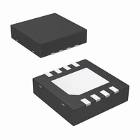
DS10BR150TSD/NOPB National Semiconductor, DS10BR150TSD/NOPB Datasheet - Page 4

DS10BR150TSD/NOPB
Manufacturer Part Number
DS10BR150TSD/NOPB
Description
IC BUFFER/REPEATER LVDS 8-LLP
Manufacturer
National Semiconductor
Type
Bufferr
Datasheet
1.DS10BR150TSDNOPB.pdf
(12 pages)
Specifications of DS10BR150TSD/NOPB
Tx/rx Type
LVDS
Delay Time
380ps
Capacitance - Input
1.7pF
Voltage - Supply
3 V ~ 3.6 V
Current - Supply
21mA
Mounting Type
Surface Mount
Package / Case
8-LLP
Number Of Elements
1
Number Of Receivers
1
Number Of Drivers
1
Operating Supply Voltage (typ)
3.3V
Differential Input High Threshold Voltage
100mV
Diff. Input Low Threshold Volt
-100mV
Output Type
Repeater
Differential Output Voltage
450mV
Transmission Data Rate
1000Mbps
Propagation Delay Time
0.6ns
Power Dissipation
2.08W
Operating Temp Range
-40C to 85C
Operating Temperature Classification
Industrial
Mounting
Surface Mount
Pin Count
8
Data Rate
1 Gbps
Operating Supply Voltage
3.3 V
Maximum Power Dissipation
2080 mW
Maximum Operating Temperature
+ 85 C
Minimum Operating Temperature
- 40 C
Mounting Style
SMD/SMT
Supply Voltage (max)
3.6 V
Supply Voltage (min)
3 V
Supply Current
21mA
Supply Voltage Range
3V To 3.6V
Driver Case Style
LLP
No. Of Pins
8
Operating Temperature Range
-40°C To +85°C
Msl
MSL 3 - 168 Hours
Filter Terminals
SMD
Logic Type
Buffer
Rohs Compliant
Yes
Data Rate Max
1Gbps
For Use With
DS10BR150EVK - BOARD EVALUATION DS10BR150
Lead Free Status / RoHS Status
Lead free / RoHS Compliant
Other names
DS10BR150TSD
DS10BR150TSDTR
DS10BR150TSDTR
Available stocks
Company
Part Number
Manufacturer
Quantity
Price
Company:
Part Number:
DS10BR150TSD/NOPB
Manufacturer:
LT
Quantity:
300
www.national.com
Symbol
LVDS OUTPUT AC SPECIFICATIONS (OUT+, OUT-)
t
t
t
t
t
t
JITTER PERFORMANCE (Figure 5)
t
t
t
PHLD2
PLHD2
SKD1
SKD2
LHT
HLT
DJ
RJ
TJ
AC Electrical Characteristics
Over recommended operating supply and temperature ranges unless otherwise specified. (Notes 5, 7)
Note 4: “Absolute Maximum Ratings” indicate limits beyond which damage to the device may occur, including inoperability and degradation of device reliability
and/or performance. Functional operation of the device and/or non-degradation at the Absolute Maximum Ratings or other conditions beyond those indicated in
the Recommended Operating Conditions is not implied. The Recommended Operating Conditions indicate conditions at which the device is functional and the
device should not be operated beyond such conditions.
Note 5: The Electrical Characteristics tables list guaranteed specifications under the listed Recommended Operating Conditions except as otherwise modified
or specified by the Electrical Characteristics Conditions and/or Notes. Typical specifications are estimations only and are not guaranteed.
Note 6: Current into device pins is defined as positive. Current out of device pins is defined as negative. All voltages are referenced to ground except V
ΔV
Note 7: Typical values represent most likely parametric norms for V
product characterization and are not guaranteed.
Note 8: Output short circuit current (I
Note 9: Specification is guaranteed by characterization and is not tested in production.
Note 10: t
the same channel.
Note 11: t
applies to devices at the same V
Note 12: Measured on a clock edge with a histogram and an acummulation of 1500 histogram hits. Input stimulus jitter is subtracted geometrically.
Note 13: Tested with a combination of the 1100000101 (K28.5+ character) and 0011111010 (K28.5- character) patterns. Input stimulus jitter is subtracted
algebraically.
Note 14: Measured on an eye diagram with a histogram and an acummulation of 3500 histogram hits. Input stimulus jitter is subtracted.
OD
.
Differential Propagation Delay High to Low
Differential Propagation Delay Low to High
Pulse Skew |t
Part to Part Skew (Note 11)
Rise Time
Fall Time
Deterministic Jitter (Peak-to-Peak Value )
(Note 13)
Random Jitter (RMS Value)
(Note 12)
Total Jitter (Peak to Peak Value)
(Note 14)
SKD1
SKD2
, |t
, Part to Part Skew, is defined as the difference between the minimum and maximum specified differential propagation delays. This specification
PLHD
− t
PHLD
PLHD
|, is the magnitude difference in differential propagation delay time between the positive going edge and the negative going edge of
− t
CC
Parameter
PHLD
and within 5°C of each other within the operating temperature range.
OS
) is specified as magnitude only, minus sign indicates direction only.
| (Note 10)
(Note 9)
CC
= +3.3V and T
R
R
V
V
K28.5 (NRZ)
V
V
Clock (NRZ)
V
V
PRBS-23 (NRZ)
ID
CM
ID
CM
ID
CM
L
L
= 100Ω
= 100Ω
= 350 mV
= 350 mV
= 350 mV
= 1.2V
= 1.2V
= 1.2V
4
A
= +25°C, and at the Recommended Operation Conditions at the time of
Conditions
622 Mbps
1.06 Gbps
311 MHz
503 MHz
622 Mbps
1.06 Gbps
Min
0.02
0.02
Typ
380
410
165
155
0.6
0.6
30
45
12
15
Max
0.04
0.05
600
600
150
160
400
400
1.3
1.1
39
42
OD
Units
and
UI
UI
ps
ps
ps
ps
ps
ps
ps
ps
ps
ps
P-P
P-P


