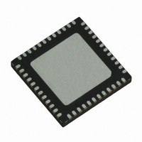
PI2EQX4432DZDE Pericom Semiconductor, PI2EQX4432DZDE Datasheet - Page 3

PI2EQX4432DZDE
Manufacturer Part Number
PI2EQX4432DZDE
Description
IC PCI-E REPEATER 48TQFN
Manufacturer
Pericom Semiconductor
Type
Repeaterr
Datasheet
1.PI2EQX4432DZDE.pdf
(6 pages)
Specifications of PI2EQX4432DZDE
Tx/rx Type
CML
Voltage - Supply
1.7 V ~ 1.9 V
Mounting Type
Surface Mount
Package / Case
48-TQFN
Lead Free Status / RoHS Status
Lead free / RoHS Compliant
Current - Supply
-
Delay Time
-
Capacitance - Input
-
Lead Free Status / Rohs Status
Details
Available stocks
Company
Part Number
Manufacturer
Quantity
Price
Company:
Part Number:
PI2EQX4432DZDE
Manufacturer:
Pericom
Quantity:
126
Part Number:
PI2EQX4432DZDE
Manufacturer:
PERICOM
Quantity:
20 000
Output Swing Control
AC/DC Electrical Characteristics
Notes
1.
2.
Maximum Ratings
(Above which useful life may be impaired. For user guide lines, not tested.)
Ps
CML Receiver Input
RL
V
V
V
Z
Z
Equalization
J
J
3, 6, 9, 12, 28, 31,
SEL–OL_[A:D]
RS
RM
RX-DIFF-DC
RX-DC
Storage Temperature ........................................................ –65°C to +150°C
Supply Voltage to Ground Potential ................................... –0.5V to +2.5V
DC SIG Voltage ..........................................................–0.5V to V
Current Output ................................................................-25mA to +25mA
Power Dissipation Continous ......................................................... 800mW
Operating Temperature .............................................................. 0 to +70°C
RX-DIFFP-P
RX-CM-ACP
TH
25, Center Pad
RX
K28.7 pattern is applied differentially at point A as shown in Figure 1.
Total jitter does not include the signal source jitter. Total jitter (TJ) = (14.1 × RJ + DJ) where RJ is random RMS jitter and DJ is maximum
deterministic jitter. Signal source is a K28.5 ± pattern (00 1111 1010 11 0000 0101) for the deterministic jitter test and K28.7 (0011111000) or
equivalent for random jitter test. Residual jitter is that which remains after equalizing media-induced losses of the environment of Figure 1 or
its equivalent. The deterministic jitter at point B must be from media-induced loss, and not from clock source modulation. Jitter is measured at
0V at point C of Figure 1.
Symbol
34, 37, 48
-
07-0106
24
0
1
Supply Power
Latency
Return Loss
Differential Input Peak-to-
peak Voltage
AC Peak Common Mode
Input Voltage
Signal Detect Threshold
DC Differential Input
Impedance
DC Input Impedance
Residual Jitter
Random Jitter
Output Swing
IREF
VDD
GND
Parameter
1.2x
1x
(1,2)
(1,2)
PWR
PWR
I
Output De-emphasis Adjustment
SEL−DE_[A:D]
(V
Connect to 475-Ohm resistor to ground when the reference clock is used. Otherwise
do not connect.
1.8V Supply Voltage
Supply Ground, Center pad must be connected
DD
All Enables = LVCMOS High
All Enables = LVCMOS Low
From input to output
50 MHz to 1.25 GHz
EN_x = High
Total Jitter
Deterministic jitter
= 1.8 ±0.1V)
0
1
De-emphasis
Conditions
3
DD
–3.5dB
2.5Gbps x2 Lane PCI Express Repeater / Equalizer
0dB
+0.5V
with Signal Detect and Flow-through Pinout
Note:
Stresses greater than those listed under MAX I MUM RAT-
INGS may cause permanent damage to the de vice. This is
a stress rating only and func tion al op er a tion of the device
at these or any other conditions above those indicated in
the operational sections of this spec i fi ca tion is not implied.
Exposure to absolute max i mum rating con di tions for ex-
tended periods may affect re li abil i ty.
Equalizer Selection
SEL−EQ_[A:D]
0
1
0.175
Min.
80
40
Typ.
120
100
2.0
1.5
12
50
Compliance Channel
[0:2.5dB] @ 1.25 GHz
[0:6.5dB] @ 1.25 GHz
PI2EQX4432D
1.200
PS8888A
Max.
150
175
120
0.1
0.6
0.3
0.2
60
psrms
Units
Ulp-p
mV
mV
dB
W
ns
V
Ω
04/26/07


