DS33X11+ Maxim Integrated Products, DS33X11+ Datasheet - Page 6
DS33X11+
Manufacturer Part Number
DS33X11+
Description
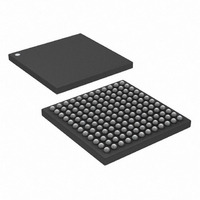
IC MAPPING ETHERNET 144CSBGA
Manufacturer
Maxim Integrated Products
Datasheet
1.DS33X11.pdf
(375 pages)
Specifications of DS33X11+
Applications
Data Transport
Interface
SPI
Voltage - Supply
1.8V, 2.5V, 3.3V
Package / Case
144-CSBGA
Mounting Type
Surface Mount
Lead Free Status / RoHS Status
Lead free / RoHS Compliant


________________________________________________ DS33X162/X161/X82/X81/X42/X41/X11/W41/W11
List of Figures
Figure 3-1. Standardized Ethernet Transport over Multiple T1/E1 Lines .................................................................. 14
Figure 3-2. Standardized Ethernet Transport over a Single T1/E1 Line ................................................................... 15
Figure 3-3. Remote IP DSLAM T1/E1 Trunk Card .................................................................................................... 16
Figure 6-1. Simplified Logical Block Diagram............................................................................................................ 20
Figure 7-1. 256-Ball, 17mm x 17mm CSBGA Pinout (DS33X162/X161/X82/X81/X42/X41) .................................... 31
Figure 7-2. 256-Ball, 17mm x 17mm CSBGA Pinout (DS33W41/DS33W11)........................................................... 32
Figure 7-3. 144-Ball, 10mm x 10mm, CSBGA Pinout (DS33X11) ............................................................................ 33
Figure 8-1. Clocking Diagram .................................................................................................................................... 38
Figure 8-2. Device Interrupt Information Flow Diagram ............................................................................................ 42
Figure 8-3. Forwarding Mode 1: Single Ethernet Port with Priority Forwarding ........................................................ 44
Figure 8-4. Forwarding Mode 2: One or Two Ethernet Port Forwarding with Scheduling......................................... 45
Figure 8-5. Forwarding Mode 3: Single Ethernet Port with LAN-VLAN Forwarding.................................................. 46
Figure 8-6. Forwarding Mode 4: 1 Ethernet port with Port ID and LAN-VLAN Forwarding....................................... 47
Figure 8-7. Forwarding Mode 5: Full LAN-to-WAN and WAN-to-LAN VLAN Forwarding ......................................... 48
Figure 8-8. IEEE 802.3 Ethernet Frame .................................................................................................................... 60
Figure 8-9. Example Configuration of GMII Interface (DTE Mode Only)................................................................... 62
Figure 8-10. Example Configuration as DTE connected to an Ethernet PHY in MII Mode ....................................... 63
Figure 8-11. Example Configuration as a DCE in MII Mode ..................................................................................... 65
Figure 8-12. RMII Interface (DTE Mode Only)........................................................................................................... 66
Figure 8-13. IEEE 802.1Q and 802.1p Field Format ................................................................................................. 69
Figure 8-14. VLAN Q-in-Q Field Format.................................................................................................................... 70
Figure 8-15. Differentiated Services Code Point (DSCP) Header Information.......................................................... 71
Figure 8-16. Supported Trapped Ethernet Frame Types .......................................................................................... 75
Figure 8-17. MII Management Frame ........................................................................................................................ 83
Figure 8-18. GFP-F NULL Encapsulated Frame Format .......................................................................................... 91
Figure 8-19. GFP-F LINEAR EXTENSION Encapsulated Frame Format................................................................. 93
Figure 8-20. LAPS / X.86 Encapsulated Frame Format ............................................................................................ 94
Figure 8-21. HDCL Encapsulated Frame Format...................................................................................................... 97
Figure 8-22. cHDLC Encapsulated Frame Format .................................................................................................... 98
Figure 9-1. Interfacing with T1/E1 Transceivers...................................................................................................... 101
Figure 9-2. Example Functional Timing: DS2155 E1 Transmit-Side Boundary Timing .......................................... 101
Figure 9-3. Example Functional Timing: DS2155 T1 Transmit-Side Boundary Timing........................................... 102
Figure 9-4. Example Functional Timing: DS2155 E1 Receive-Side Boundary Timing ........................................... 102
Figure 9-5. Example Functional Timing: DS2155 T1 Receive-Side Boundary Timing............................................ 102
Figure 9-6. Interfacing with T3/E3 Transceivers...................................................................................................... 103
Figure 9-7. Example Functional Timing: DS3170 DS3 Transmit-Side Boundary Timing........................................ 103
Figure 9-8. Example Functional Timing: DS3170 DS3 Receive-Side Boundary Timing......................................... 104
Figure 11-1. SPI Serial Port Access For Read Mode, SPI_CPOL=0, SPI_CPHA = 0 ............................................ 330
Figure 11-2. SPI Serial Port Access For Read Mode, SPI_CPOL = 1, SPI_CPHA = 0 .......................................... 330
Figure 11-3. SPI Serial Port Access For Read Mode, SPI_CPOL = 0, SPI_CPHA = 1 .......................................... 331
Figure 11-4. SPI Serial Port Access For Read Mode, SPI_CPOL = 1, SPI_CPHA = 1 .......................................... 331
Figure 11-5. SPI Serial Port Access For Write Mode, SPI_CPOL = 0, SPI_CPHA = 0 .......................................... 331
Figure 11-6. SPI Serial Port Access For Write Mode, SPI_CPOL = 1, SPI_CPHA = 0 .......................................... 331
Figure 11-7. SPI Serial Port Access For Write Mode, SPI_CPOL = 0, SPI_CPHA = 1 .......................................... 332
Figure 11-8. SPI Serial Port Access For Write Mode, SPI_CPOL = 1, SPI_CPHA = 1 .......................................... 332
Figure 11-9. Transmit Serial Port Interface, without VCAT ..................................................................................... 333
Figure 11-10. Transmit Serial Port Interface with VCAT ......................................................................................... 333
Figure 11-11. Transmit Serial Port Interface, with Gapped Clock ........................................................................... 333
Figure 11-12. Transmit Serial Port Interface with VCAT, early TSYNC (2 cycles).................................................. 334
Figure 11-13. Receive Serial Port Interface, without VCAT, rising edge sampling ................................................. 334
Figure 11-14. Receive Serial Port Interface with VCAT, rising edge sampling ....................................................... 334
Figure 11-15. Receive Serial Port Interface with Gapped Clock (T1) ..................................................................... 334
Figure 11-16. Transmit Voice Port Interface with PCM Octets................................................................................ 335
Figure 11-17. Receive Voice Port Interface with PCM Octets................................................................................. 335
Figure 11-18. GMII Transmit Interface Functional Timing ....................................................................................... 336
Rev: 063008
6 of 375
Related parts for DS33X11+
Image
Part Number
Description
Manufacturer
Datasheet
Request
R

Part Number:
Description:
MAX7528KCWPMaxim Integrated Products [CMOS Dual 8-Bit Buffered Multiplying DACs]
Manufacturer:
Maxim Integrated Products
Datasheet:
Part Number:
Description:
Single +5V, fully integrated, 1.25Gbps laser diode driver.
Manufacturer:
Maxim Integrated Products
Datasheet:
Part Number:
Description:
Single +5V, fully integrated, 155Mbps laser diode driver.
Manufacturer:
Maxim Integrated Products
Datasheet:
Part Number:
Description:
VRD11/VRD10, K8 Rev F 2/3/4-Phase PWM Controllers with Integrated Dual MOSFET Drivers
Manufacturer:
Maxim Integrated Products
Datasheet:
Part Number:
Description:
Highly Integrated Level 2 SMBus Battery Chargers
Manufacturer:
Maxim Integrated Products
Datasheet:
Part Number:
Description:
Current Monitor and Accumulator with Integrated Sense Resistor; ; Temperature Range: -40°C to +85°C
Manufacturer:
Maxim Integrated Products
Part Number:
Description:
TSSOP 14/A�/RS-485 Transceivers with Integrated 100O/120O Termination Resis
Manufacturer:
Maxim Integrated Products
Part Number:
Description:
TSSOP 14/A�/RS-485 Transceivers with Integrated 100O/120O Termination Resis
Manufacturer:
Maxim Integrated Products
Part Number:
Description:
QFN 16/A�/AC-DC and DC-DC Peak-Current-Mode Converters with Integrated Step
Manufacturer:
Maxim Integrated Products
Part Number:
Description:
TDFN/A/65V, 1A, 600KHZ, SYNCHRONOUS STEP-DOWN REGULATOR WITH INTEGRATED SWI
Manufacturer:
Maxim Integrated Products
Part Number:
Description:
Integrated Temperature Controller f
Manufacturer:
Maxim Integrated Products
Part Number:
Description:
SOT23-6/I�/45MHz to 650MHz, Integrated IF VCOs with Differential Output
Manufacturer:
Maxim Integrated Products
Part Number:
Description:
SOT23-6/I�/45MHz to 650MHz, Integrated IF VCOs with Differential Output
Manufacturer:
Maxim Integrated Products
Part Number:
Description:
EVALUATION KIT/2.4GHZ TO 2.5GHZ 802.11G/B RF TRANSCEIVER WITH INTEGRATED PA
Manufacturer:
Maxim Integrated Products
Part Number:
Description:
QFN/E/DUAL PCIE/SATA HIGH SPEED SWITCH WITH INTEGRATED BIAS RESISTOR
Manufacturer:
Maxim Integrated Products
Datasheet: