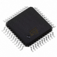
PSD303B-70M STMicroelectronics, PSD303B-70M Datasheet - Page 19

PSD303B-70M
Manufacturer Part Number
PSD303B-70M
Description
MCU 8BIT PROGRM 70NS 44-PQFP
Manufacturer
STMicroelectronics
Datasheet
1.PSD303B-70M.pdf
(85 pages)
Specifications of PSD303B-70M
Applications
*
Interface
*
Voltage - Supply
*
Package / Case
44-MQFP, 44-PQFP
Mounting Type
Surface Mount
Lead Free Status / RoHS Status
Lead free / RoHS Compliant
Available stocks
Company
Part Number
Manufacturer
Quantity
Price
Company:
Part Number:
PSD303B-70M
Manufacturer:
STMicroelectronics
Quantity:
10 000
10.0
I/O Port
Functions
(
16
PSD3XX Family
PSD3XX Family
cont.)
10.2 Port A (PA0-PA7)
The control registers of Port A are located in CSIOPORT space; see Table 5.
10.2.1 Port A (PA0-PA7) in Multiplexed Address/Data Mode
Each pin of Port A can be individually configured. The following table summarizes what the
control registers (in CSIOPORT space) for Port A do:
MCU I/O Mode
The default configuration of Port A is MCU I/O. In this mode, every pin can be set (at run-
time) as an input or output by writing to the respective pin’s direction flip-flop (DIR FF,
Figure 5A). As an output, the pin level can be controlled by writing to the respective pin’s
data flip-flop (DFF, Figure 5A). The Pin Register can be read to determine logic level of the
pin. The contents of the Pin Register indicate the true state of the PSD driving the pin
through the DFF or an external source driving the pin. Pins can be configured as CMOS
or open-drain using ST’s PSDsoft software. Open-drain pins require external pull-up
resistors.
Latched Address Output Mode
Alternatively, any bit(s) of Port A can be configured to output low-order demultiplexed
address bus bit. The address is provided by the internal PSD address latch, which latches
the address on the trailing edge of ALE/AS. Port A then outputs the desired demultiplexed
address bits. This feature can eliminate the need for an external latch (for example:
74LS373) if you have devices that require low-order latched address bits. Although any pin
of Port A may output an address signal, the pin is position-dependent. In other words, pin
PA0 of Port A may only pass A0, PA1 only A1, and so on.
Track Mode
Track Mode sets the entire port to track the signals on AD0/A0-AD7/A7, depending on
specific address ranges defined by the PAD’s CSADIN, CSADOUT1, and CSADOUT2
signals. This feature lets the user interface the microcontroller to shared external resources
without requiring external buffers and decoders. In Track Mode, Port A effectively operates
as a bi-directional buffer, allowing external MCUs or host processors to access the local
data bus. Keep the following information in mind when setting up Track Mode:
NOTE: 1. Default value is the value after reset.
Port A Pin Register
Port A Direction Register
Port A Data Register
The direction is controlled by:
•
•
•
•
When CSADOUT1 and ALE/AS are true, the address on AD0/A0-AD7/A7 is output on
Port A. Note: carefully check the generation of CSADOUT1 to ensure that it is stable
during the ALE/AS pulse.
When CSADOUT2 is active and a write operation is performed, the data on the
AD0/A0-AD7/A7 input pins flows out through Port A.
When CSADIN is active and a read operation is performed, the data on Port A flows
out through the AD0/A0-AD7/A7 pins.
Port A is tri-stated when none of the above conditions exist.
ALE/AS
RD/E or RD/E/DS (DS on non-3X1 devices only)
WR or R/W
PAD outputs CSADOUT1, CSADOUT2, and CSADIN defined in PSDsoft design.
Register Name
Sampled logic level
Data in DFF = ‘0’
Pin is configured
at pin = ‘0’
0 Value
as input
Sampled logic level
Data in DFF = ‘1’
Pin is configured
at pin = ‘1’
as output
1 Value
Default
Value
(Note 1)
X
0
0


