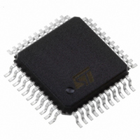
PSD303B-70M STMicroelectronics, PSD303B-70M Datasheet - Page 25

PSD303B-70M
Manufacturer Part Number
PSD303B-70M
Description
MCU 8BIT PROGRM 70NS 44-PQFP
Manufacturer
STMicroelectronics
Datasheet
1.PSD303B-70M.pdf
(85 pages)
Specifications of PSD303B-70M
Applications
*
Interface
*
Voltage - Supply
*
Package / Case
44-MQFP, 44-PQFP
Mounting Type
Surface Mount
Lead Free Status / RoHS Status
Lead free / RoHS Compliant
Available stocks
Company
Part Number
Manufacturer
Quantity
Price
Company:
Part Number:
PSD303B-70M
Manufacturer:
STMicroelectronics
Quantity:
10 000
12.0
Control Signals
22
PSD3XX Family
Table 6. Truth Table for BHE and Address Bit A0 (16-bit MCUs only)
Consult your MCU data sheet to determine which control signals your MCU generates, and
how they operate. This section is intended to show which control signals should be
connected to what pins on the PSD3XX. You will then use PSDsoft to configure the
PSD3XX, based on the combination of control signals that your MCU outputs, for example
RD, WR, and PSEN.
The PSD3XX is compatible with the following control signals:
12.1 ALE or AS
Connect the ALE or AS signal from your MCU to this pin where applicable, and program
the polarity using PSDsoft. The trailing edge (when the signal goes inactive) of ALE or AS
latches the address on any pins that have an address input. If you are using a
non-multiplexed-bus MCU that does not output an ALE or AS signal, this pin can be used
for a generic input to the PAD. Note: if your data is multiplexed with address lines other
than A0-A7, connect your address pins to AD0/A0-AD15/A15, and connect your data to
Port A (and Port B where applicable), and connect the ALE/AS signal to this pin.
12.2 WR or R/W
Your MCU should output a stand-alone write signal (WR) or a multiplexed read/write signal
(R/W). In either case, the signal should be connected to this pin.
12.3 RD/E/DS (DS option not available on 3X1 devices)
Your MCU should output any one of RD, E (clock), or DS. In any case, connect the
appropriate signal to this pin.
12.4 BHE or PSEN
•
•
•
•
•
•
If your MCU does not output either of these signals, tie this pin to Vcc
(through a series resistor), and skip to the next signal.
If you use an 8-bit 8031 compatible MCU that outputs a separate signal when
accessing program space, such as PSEN, connect it to this pin. You would then use
PSDsoft to configure the EPROM in the PSD3XX to respond to PSEN only or PSEN
and RD. If you have an 8031 compatible MCU, refer to the “Program/Data Space and
the 8031” section for further information.
If you are using a 16-bit MCU, connect the BHE (or similar signal) output to this pin.
BHE enables accessing of the upper byte of the data bus. See Table 6 for information
on how this signal is used in conjunction with the A0 address line.
ALE or AS (polarity is programmable)
WR or R/W
RD/E or RD/E/DS (DS for non-3X1 devices only)
BHE or PSEN
A19/CSI
RESET (polarity is programmable except on low voltage versions with the V suffix).
BHE
0
0
1
1
A
0
1
0
1
0
Whole Word
Upper Byte From/To Odd Address
Lower Byte From/To Even Address
None
Operation


