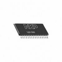
UJA1065TW/5V0,518 NXP Semiconductors, UJA1065TW/5V0,518 Datasheet - Page 44

UJA1065TW/5V0,518
Manufacturer Part Number
UJA1065TW/5V0,518
Description
IC CAN/LIN FAIL-SAFE 32HTSSOP
Manufacturer
NXP Semiconductors
Datasheet
1.UJA1065TW3V3CT.pdf
(76 pages)
Specifications of UJA1065TW/5V0,518
Package / Case
32-TSSOP Exposed Pad, 32-eTSSOP, 32-HTSSOP
Applications
Networking
Interface
CAN, LIN
Voltage - Supply
5.5 V ~ 52 V
Mounting Type
Surface Mount
Product
Controller Area Network (CAN)
Number Of Transceivers
1
Data Rate
20 Kbps
Supply Voltage (max)
27 V, 52 V
Supply Voltage (min)
5.5 V
Supply Current (max)
10 mA
Maximum Operating Temperature
+ 125 C
Minimum Operating Temperature
- 40 C
Mounting Style
SMD/SMT
Lead Free Status / RoHS Status
Lead free / RoHS Compliant
Other names
568-4374-2
935281292518
UJA1065TW/5V0-T
UJA1065TW/5V0-T
935281292518
UJA1065TW/5V0-T
UJA1065TW/5V0-T
NXP Semiconductors
Table 22.
Table 23.
Table 24.
UJA1065_7
Product data sheet
Symbol
ISDM
ERREM
WDPRE
V1RTHC
Symbol
DIC
GP0[10:7]
GP0[6:0]
Symbol
GP1[11:0]
Special Mode register: status at reset
General Purpose register 0 and General Purpose Feedback register 0: status at reset
General Purpose register 1 and General Purpose Feedback register 1: status at reset
Name
Initialize Software Development Mode
Error pin emulation mode
Watchdog Prescale Factor
V1 Reset Threshold Control
Name
Device Identification Control
general purpose bits 10 to 7 (version)
general purpose bits 6 to 0 (SBC type)
Name
general purpose bits 11 to 0
6.14.1 Software development mode
6.14 Test modes
The Software development mode is intended to support software developers in writing
and pretesting application software without having to work around watchdog triggering
and without unwanted jumps to Fail-safe mode.
In Software development mode the following events do not force a system reset:
However, in case of a watchdog trigger failure the reset source information is still provided
in the System Status register as if there was a real reset event.
The exclusion of watchdog related resets allows simplified software testing, because
possible problems in the watchdog triggering can be indicated by interrupts instead of
resets. The SDM bit does not affect the watchdog behavior in Standby and Sleep mode.
This allows the cyclic wake-up behavior to be evaluated during Standby and Sleep mode
of the SBC.
All transitions to Fail-safe mode are disabled. This allows working with an external
emulator that clamps the reset line LOW in debugging mode. A V1 undervoltage of more
than t
SBC). Transitions from Start-up mode to Restart mode are still possible.
•
•
•
•
Watchdog overflow in Normal mode
Watchdog window miss
Interrupt time-out
Elapsed start-up time
V1(CLT)
is the only exception that results in entering Fail-safe mode (to protect the
Rev. 07 — 25 February 2010
0 (no)
0 (EN function)
00 (90 %)
0 (Device ID)
000 0101 (UJA1065) no change
0000 0000 0000
Power-on
00 (factor 1)
Power-on
Mask version
Power-on
High-speed CAN/LIN fail-safe system basis chip
no change
no change
no change
no change
no change
no change
no change
Start-up
Start-up
Start-up
no change
no change
no change
00 (90 %)
no change
no change
no change
Restart
Restart
no change
Restart
UJA1065
© NXP B.V. 2010. All rights reserved.
44 of 76


