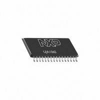
UJA1065TW/5V0,518 NXP Semiconductors, UJA1065TW/5V0,518 Datasheet - Page 55

UJA1065TW/5V0,518
Manufacturer Part Number
UJA1065TW/5V0,518
Description
IC CAN/LIN FAIL-SAFE 32HTSSOP
Manufacturer
NXP Semiconductors
Datasheet
1.UJA1065TW3V3CT.pdf
(76 pages)
Specifications of UJA1065TW/5V0,518
Package / Case
32-TSSOP Exposed Pad, 32-eTSSOP, 32-HTSSOP
Applications
Networking
Interface
CAN, LIN
Voltage - Supply
5.5 V ~ 52 V
Mounting Type
Surface Mount
Product
Controller Area Network (CAN)
Number Of Transceivers
1
Data Rate
20 Kbps
Supply Voltage (max)
27 V, 52 V
Supply Voltage (min)
5.5 V
Supply Current (max)
10 mA
Maximum Operating Temperature
+ 125 C
Minimum Operating Temperature
- 40 C
Mounting Style
SMD/SMT
Lead Free Status / RoHS Status
Lead free / RoHS Compliant
Other names
568-4374-2
935281292518
UJA1065TW/5V0-T
UJA1065TW/5V0-T
935281292518
UJA1065TW/5V0-T
UJA1065TW/5V0-T
NXP Semiconductors
Table 26.
T
voltages are defined with respect to ground. Positive currents flow into the IC.
[1]
[2]
[3]
[4]
UJA1065_7
Product data sheet
Symbol
ΔV
I
I
TEST input; pin TEST
V
R
Temperature detection
T
RTLIN(pu)
LL
vj
j(warn)
th(TEST)
(pd)TEST
=
RTLIN
All parameters are guaranteed over the virtual junction temperature range by design. Products are 100 % tested at 125 °C ambient
temperature on wafer level (pretesting). Cased products are 100 % tested at 25 °C ambient temperature (final testing). Both pretesting
and final testing use correlated test conditions to cover the specified temperature and power supply voltage range.
V
Not tested in production.
V2 internally supplies the SBC CAN transceiver. The supply current needed for the CAN transceiver reduces the pin V2 output
capability. The performance of the CAN transceiver can be impaired if V2 is also used to supply other circuitry while the CAN transceiver
is in use.
−
V1(nom)
40
°
C to +150
Static characteristics
is 3.3 V or 5 V, depending on the SBC version.
Parameter
RTLIN load
regulation
RTLIN pull-up
current
LOW-level leakage
current
input threshold
voltage
pull-down resistor
high junction
temperature warning
level
°
C, V
BAT42
= 5.5 V to 52 V; V
…continued
Conditions
Active mode;
I
V
Active mode;
V
t > t
Off-line mode;
V
t < t
Off-line mode;
V
t > t
for entering Software
development mode;
T
for entering Forced normal
mode; T
between pin TEST and GND
RTLIN
j
BAT42
RTLIN
RTLIN
RTLIN
= 25 °C
LIN(dom)(det)
LIN(dom)(det)
LIN(dom)(det)
Rev. 07 — 25 February 2010
BAT14
= −10 μA to −10 mA;
= V
= V
= V
= 7 V to 27 V
j
= 25 °C
LIN
LIN
LIN
= 5.5 V to 27 V; V
= 0 V;
= 0 V;
= 0 V;
High-speed CAN/LIN fail-safe system basis chip
BAT42
[1]
≥
2
Min
-
−150
−150
−10
1
2
160
V
BAT14
−
1 V; unless otherwise specified. All
Typ
0.65
−60
−60
0
5
10
4
175
UJA1065
8
Max
2
−35
−35
+10
8
13.5
190
© NXP B.V. 2010. All rights reserved.
kΩ
Unit
V
μA
μA
μA
V
V
°C
55 of 76


