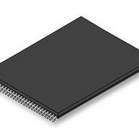
S29GL256S10TFI010 Spansion Inc., S29GL256S10TFI010 Datasheet - Page 73

S29GL256S10TFI010
Manufacturer Part Number
S29GL256S10TFI010
Description
Flash 256 MBIT 3V 100NS PAGE MODE FLASH
Manufacturer
Spansion Inc.
Datasheet
1.S29GL256S10TFI010.pdf
(97 pages)
Specifications of S29GL256S10TFI010
Data Bus Width
16 bit
Memory Type
Flash
Memory Size
256 Mbit
Architecture
Uniform
Timing Type
Asynchronous
Interface Type
CFI
Access Time
100 ns
Supply Voltage (max)
3.6 V
Supply Voltage (min)
2.7 V
Maximum Operating Current
100 mA
Operating Temperature
- 40 C to + 85 C
Mounting Style
SMD/SMT
Package / Case
TSOP-56
Lead Free Status / Rohs Status
Compliant
Available stocks
Company
Part Number
Manufacturer
Quantity
Price
Company:
Part Number:
S29GL256S10TFI010
Manufacturer:
Spansion
Quantity:
25
9.4
February 11, 2011 S29GL_128S_01GS_00_01
DC Characteristics
Notes:
1. I
2. Not 100% tested.
3. Automatic sleep mode enables the lower power mode when addresses remain stable for t
4. V
5. V
6. During power-up there are spikes of current demand, the system needs to be able to supply this current to insure the part initializes
7. If an embedded operation is in progress at the start of reset, the current consumption will remain at the embedded operation specification
8. The recommended pull-up resistor for RY/BY# output is 5K to 10K Ohms.
Parameter
correctly.
until the embedded operation is stopped by the reset. If no embedded operation is in progress when reset is started, or following the
stopping of an embedded operation, I
mode until the next read or write.
V
V
CC
I
I
I
I
I
I
I
V
V
D a t a
I
V
V
IO
CC
CC1
CC2
CC3
CC4
CC5
CC6
CC7
I
LKO
RST
LO
OH
LI
OL
IH
IL
active while Embedded Algorithm is in progress.
= 1.65V to 3.6V or 2.7V to 3.6V depending on the model.
= 3V and V
Input Load Current
Output Leakage Current
V
V
V
Current (Notes 1, 2)
VCC Standby Current
V
Automatic Sleep Mode
V
(Notes 2, 6)
Input Low Voltage
Input High Voltage
Output Low Voltage (Notes 4, 8)
Output High Voltage
Low V
(Note 2)
Low V
(Note 2)
CC
CC
CC
CC
CC
S h e e t
Active Read Current
Intra-Page Read Current
Active Erase/Program
Reset Current (Notes 2, 7)
Current during power up
IO
CC
CC
= 3V or 1.8V. When V
Lock-Out Voltage
Power on Reset Voltage
Description
(Note 4)
(Note 4)
( A d v a n c e
(Note 4)
(Note 3)
CC7
IO
GL-S MirrorBit
will be drawn during the remainder of t
is at 1.8V, I/O pins cannot operate at >1.8V.
V
V
CE# = V
switching@ 5 MHz, V
CE# = V
switching@ 33 MHz, V
CE# = V
CE#, RESET#, OE# = V
V
CE# = V
V
V
V
V
V
RESET# = V
V
I
I
I
Table 9.3 DC Characteristics
OL
OL
OH
IN
OUT
IL
CC
IH
CC
IH
CC
CC
= V
= 100 µA for DQ15-DQ0;
= 2 mA for RY/BY#
= V
= V
= V
= 100 µA
= V
= V
= V
= V
= V
I n f o r m a t i o n )
SS
IO
IO
SS
CC
CC
CC
CC
IL
IL
IL
IH
, V
, V
SS
, V
, OE# = V
, OE# = V
, OE# = V
, RESET# = V
to V
®
max
max, t
max, t
max,
IL
IL
CC
to V
Test Conditions
IO,
Family
= V
= V
CC
= V
CE# = V
CC
, V
SS
SS
ACC
ASSB
, V
CC
CC
,
IH
IH
IH
,
CC
CC
, Address
, Address
, V
max
+ 30 ns
CC
= V
IH
IO
CC
IL
= V
= V
= V
,
, V
, OE# = V
CC
= V
CC
CC
IH
CC
max
CC
max
= V
max
max
RPH
max
IO
IO
. After the end of t
,
ACC
0.7 x V
+ 30 ns.
2.25
Min
-0.5
IO
RPH
0.85 x V
(Note 2)
the device will go to standby
+0.02
+0.02
Typ
100
1.0
55
45
70
10
53
9
3
IO
0.15 x V
0.2 x V
V
IO
±1.0
±1.0
Max
100
100
150
2.5
60
25
20
80
6
+ 0.4
IO
IO
Unit
mA
mA
mA
mA
mA
mA
µA
µA
µA
µA
V
V
V
V
V
V
73


