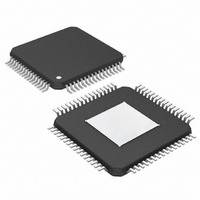
MAX4814EECB+ Maxim Integrated Products, MAX4814EECB+ Datasheet - Page 10

MAX4814EECB+
Manufacturer Part Number
MAX4814EECB+
Description
IC SW DVI/HDMI 2:4 BIDIR 64-TQFP
Manufacturer
Maxim Integrated Products
Series
4000r
Datasheet
1.MAX4814EECB.pdf
(17 pages)
Specifications of MAX4814EECB+
Function
Switch
Circuit
1 x 2:4
On-state Resistance
12 Ohm
Voltage Supply Source
Single Supply
Voltage - Supply, Single/dual (±)
4.5 V ~ 5.5 V
Current - Supply
10µA
Operating Temperature
-40°C ~ 85°C
Mounting Type
Surface Mount
Package / Case
64-TQFP Exposed Pad
Operating Supply Voltage
5 V
Supply Current
10 uA
Maximum Operating Temperature
+ 85 C
Minimum Operating Temperature
- 40 C
Mounting Style
SMD/SMT
Number Of Channels
2
Lead Free Status / RoHS Status
Lead free / RoHS Compliant
DA1 select the connections of switch A to switch SW_
and inputs DB0 and DB1. Select the connections of
switch B to SW_. See Table 3a for the pin configuration
and Table 3b for a complete summary.
In mode 1, the switch connections are controlled
through the I
registers R0 and R1. Register R0, bits [7 to 2], select
the connection of switch A and switch B to switch SW_
(see the I
The bits of register R1 transfer data to the output DO_.
The data on output DO_ is used to communicate with the
MAX3845. In mode 1, DA0/DO0 becomes output DO0,
DA1/DO1 becomes output DO1, DA2/DO2 becomes
output DO2, and DB0/DO3 becomes output DO3. DB1
and DB2 are high impedance. See Table 3a for the pin
configuration. See Table 4 for register R1 to DO_ output
mapping.
Two internal registers (RO and R1) program the
MAX4814E. Table 2 lists both registers, their address-
es, and power-up default states. Both registers are
read/write registers.
In register R0, bit BAEN is used as the enable for
switch A, and bit BBEN is used as the enable for switch
B. Writing 1 to bit BAEN enables switch A; and writing 0
to bit BAEN disables switch A. Writing 1 to bit BBEN
enables switch B, and writing 0 to bit BBEN disables
switch B. BASEL1 and BASEL0 select the connections
of switch A to switch SW_, while BBSEL1 and BBSEL0
DVI/HDMI 2:4 Low-Frequency Fanout Switch
X = Hardwired code, not programmable by user.
10
Table 1. Mode Configuration
Table 2. I
REGISTER
I
2
C Registers and Bit Descriptions
______________________________________________________________________________________
R0
R1
INPUT PIN
MODE
2
0
1
C Registers and Bit Descriptions section).
2
2
Im p ed ance
C Register Map
C interface. Inputs SDA and SCL program
BBEN
D O3
H i g h
7
Puts the device in mode 0. The direct-control inputs DA_ and DB_ control the switches.
P uts the d evi ce i n m od e 1. The sw i tches ar e contr ol l ed b y the I
Inp uts D B1 and D B2 ar e hi g h i m p ed ance.
I
2
BBSE
DO3
Data
C Interface Method (Mode 1)
L1
6
Im p ed ance
BBSEL0
DO2
High
5
BAEN
DO2
Data
4
BIT
Im p ed ance
BASEL1
DO1
High
3
select the connections of switch B to switch SW_, as
summarized in Table 6.
The two LSBs are hard coded as 00. Register R0
ignores any value written to the two LSBs; anytime reg-
ister R0 is read the hard-coded values are returned.
1 = Enable
0 = Disable
Bits BASEL1 and BASEL0 select the switch SW_ that
switch A is connected to. Bits BBSEL1 and BBSEL0
select the switch SW_ that switch B is connected to
(see Table 6).
When power is applied to the MAX4814E internal
power-on reset (POR), circuitry sets registers R0 and
R1 to their default states. Register R0 is set to all zeros,
or 00h, and register R1 is set to 10101010, or AAh, as
shown in Table 2.
Having all zeros in register R0 disables both banks A
and B; see Table 6 for register R0 to switch mapping.
Setting register R1 to AAh forces the outputs at DO_ to
be high impedance.
Note: The output, DO_ is used to communicate with the
MAX3845 when the MAX4814E is being used without its
companion. The MAX3845 and the MAX4814E use the
I
connected through a 10kΩ resistor to GND.
Bank A Enable (BAEN) and Bank B Enable (BBEN) Bits
2
C interface (MODE = 1). All DO_ outputs need to be
OPERATION
BASE
DO1
Data
L0
2
Im p ed ance
DO0
High
2
C i nter face. D O _ b ecom es an acti ve outp ut.
1
X
Bank A Select (BASEL1/BASEL0) and
Bank B Select (BBSEL1/BBSEL0) Bits
DO0
Data
Power-On Default States
0
X
I
2
C Register R0 Two LSB Bits
ADDRESS
0x00
0x01
BINARY
0000
0000
1010
1010
POWER-UP
HEX
AA
00


