MAX4814EECB+ Maxim Integrated Products, MAX4814EECB+ Datasheet - Page 7
MAX4814EECB+
Manufacturer Part Number
MAX4814EECB+
Description
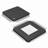
IC SW DVI/HDMI 2:4 BIDIR 64-TQFP
Manufacturer
Maxim Integrated Products
Series
4000r
Datasheet
1.MAX4814EECB.pdf
(17 pages)
Specifications of MAX4814EECB+
Function
Switch
Circuit
1 x 2:4
On-state Resistance
12 Ohm
Voltage Supply Source
Single Supply
Voltage - Supply, Single/dual (±)
4.5 V ~ 5.5 V
Current - Supply
10µA
Operating Temperature
-40°C ~ 85°C
Mounting Type
Surface Mount
Package / Case
64-TQFP Exposed Pad
Operating Supply Voltage
5 V
Supply Current
10 uA
Maximum Operating Temperature
+ 85 C
Minimum Operating Temperature
- 40 C
Mounting Style
SMD/SMT
Number Of Channels
2
Lead Free Status / RoHS Status
Lead free / RoHS Compliant


1, 16, 24, 25, 33, 48, 56, 57
8, 9, 17, 32, 40, 41, 49, 64
DVI/HDMI 2:4 Low-Frequency Fanout Switch
2, 15, 34
31, 50
PIN
10
11
12
13
14
18
19
20
21
22
23
26
27
28
29
30
35
36
37
38
39
42
43
44
3
4
5
6
7
_______________________________________________________________________________________
SW3[4]
SW3[3]
SW3[2]
SW3[1]
SW3[0]
SW2[4]
SW2[3]
SW2[2]
SW2[1]
SW2[0]
SW1[4]
SW1[3]
SW1[2]
NAME
MODE
GND
A[0]
A[1]
A[2]
A[3]
A[4]
B[0]
B[1]
B[2]
B[3]
B[4]
SDA
SCL
AD0
AD1
AD2
EFN
V
I.C.
DD
Ground. Must connect all GND pins together.
Internally Connected. Leave I.C. unconnected
Switch A I/O 0. A[0] has a 3Ω (typ) resistance to switch 5V or drain.
Switch A I/O 1. A[1] has a 12Ω (typ) resistance to switch data.
Switch A I/O 2. A[2] has a 12Ω (typ) resistance to switch data.
Switch A I/O 3. A[3] has a 12Ω (typ) resistance to switch data.
Switch A I/O 4. A[4] has a 3Ω (typ) resistance to switch 5V or drain.
Positive-Supply Voltage Input. Connect V
GND with a 0.1µF capacitor. Must connect all V
Switch B I/O 0. B[0] has a 3Ω (typ) resistance to switch 5V or drain.
Switch B I/O 1. B[1] has a 12Ω (typ) resistance to switch data.
Switch B I/O 2. B[2] has a 12Ω (typ) resistance to switch data.
Switch B I/O 3. B[3] has a 12Ω (typ) resistance to switch data.
Switch B I/O 4. B[4] has a 3Ω (typ) resistance to switch 5V or drain.
MODE Selection Input. Connect MODE to V
Connect MODE to GND (MODE = 0) to select direct-control mode.
I
I
Programmable I
selectable device address bit, LSB, LSB+1, MSB (see Figure 5).
Programmable I
selectable device address bit, LSB, LSB+1, MSB (see Figure 5).
Programmable I
selectable device address bit, LSB, LSB+1, MSB (see Figure 5).
Switch 3 I/O 4
Switch 3 I/O 3
Switch 3 I/O 2
Switch 3 I/O 1
Switch 3 I/O 0
ESD Protection. Connect EFN with an external 0.1µF capacitor to GND for ±15kV ESD
HBM protection. The capacitor from EFN to GND provides an additional discharge path
for the ESD energy.
Switch 2 I/O 4
Switch 2 I/O 3
Switch 2 I/O 2
Switch 2 I/O 1
Switch 2 I/O 0
Switch 1 I/O 4
Switch 1 I/O 3
Switch 1 I/O 2
2
2
C-Compatible Serial Data I/O
C-Compatible Serial Clock Input
2
2
2
C Address Bit. AD[0] sets the I
C Address Bit. AD[1] sets the I
C Address Bit. AD[2] sets the I
FUNCTION
DD
DD
to a +5V supply voltage. Bypass V
(MODE = 1) to select I
DD
2
2
2
C address of the device. User-
C address of the device. User-
C address of the device. User-
pins together.
Pin Description
2
C control mode.
DD
to
7
Related parts for MAX4814EECB+
Image
Part Number
Description
Manufacturer
Datasheet
Request
R

Part Number:
Description:
MAX7528KCWPMaxim Integrated Products [CMOS Dual 8-Bit Buffered Multiplying DACs]
Manufacturer:
Maxim Integrated Products
Datasheet:
Part Number:
Description:
Single +5V, fully integrated, 1.25Gbps laser diode driver.
Manufacturer:
Maxim Integrated Products
Datasheet:
Part Number:
Description:
Single +5V, fully integrated, 155Mbps laser diode driver.
Manufacturer:
Maxim Integrated Products
Datasheet:
Part Number:
Description:
VRD11/VRD10, K8 Rev F 2/3/4-Phase PWM Controllers with Integrated Dual MOSFET Drivers
Manufacturer:
Maxim Integrated Products
Datasheet:
Part Number:
Description:
Highly Integrated Level 2 SMBus Battery Chargers
Manufacturer:
Maxim Integrated Products
Datasheet:
Part Number:
Description:
Current Monitor and Accumulator with Integrated Sense Resistor; ; Temperature Range: -40°C to +85°C
Manufacturer:
Maxim Integrated Products
Part Number:
Description:
TSSOP 14/A�/RS-485 Transceivers with Integrated 100O/120O Termination Resis
Manufacturer:
Maxim Integrated Products
Part Number:
Description:
TSSOP 14/A�/RS-485 Transceivers with Integrated 100O/120O Termination Resis
Manufacturer:
Maxim Integrated Products
Part Number:
Description:
QFN 16/A�/AC-DC and DC-DC Peak-Current-Mode Converters with Integrated Step
Manufacturer:
Maxim Integrated Products
Part Number:
Description:
TDFN/A/65V, 1A, 600KHZ, SYNCHRONOUS STEP-DOWN REGULATOR WITH INTEGRATED SWI
Manufacturer:
Maxim Integrated Products
Part Number:
Description:
Integrated Temperature Controller f
Manufacturer:
Maxim Integrated Products
Part Number:
Description:
SOT23-6/I�/45MHz to 650MHz, Integrated IF VCOs with Differential Output
Manufacturer:
Maxim Integrated Products
Part Number:
Description:
SOT23-6/I�/45MHz to 650MHz, Integrated IF VCOs with Differential Output
Manufacturer:
Maxim Integrated Products
Part Number:
Description:
EVALUATION KIT/2.4GHZ TO 2.5GHZ 802.11G/B RF TRANSCEIVER WITH INTEGRATED PA
Manufacturer:
Maxim Integrated Products
Part Number:
Description:
QFN/E/DUAL PCIE/SATA HIGH SPEED SWITCH WITH INTEGRATED BIAS RESISTOR
Manufacturer:
Maxim Integrated Products
Datasheet: