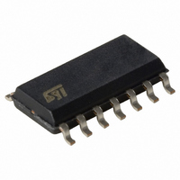
M74HC4066RM13TR STMicroelectronics, M74HC4066RM13TR Datasheet - Page 2

M74HC4066RM13TR
Manufacturer Part Number
M74HC4066RM13TR
Description
IC SWITCH QUAD 2X1 14SOIC
Manufacturer
STMicroelectronics
Series
74HCr
Type
Analog Switchr
Datasheet
1.M74HC4066TTR.pdf
(11 pages)
Specifications of M74HC4066RM13TR
Function
Switch
Circuit
4 x 2:1
On-state Resistance
80 Ohm
Voltage Supply Source
Single Supply
Voltage - Supply, Single/dual (±)
2 V ~ 12 V
Current - Supply
8µA
Operating Temperature
-55°C ~ 125°C
Mounting Type
Surface Mount
Package / Case
14-SOIC (0.154", 3.90mm Width)
Switch Configuration
SPST
On Resistance (max)
50 Ohms
On Time (max)
100 ns
Off Time (max)
115 ns
Supply Voltage (max)
12 V
Supply Voltage (min)
2 V
Maximum Power Dissipation
500 mW
Maximum Operating Temperature
+ 125 C
Mounting Style
SMD/SMT
Minimum Operating Temperature
- 55 C
Propagation Delay Time
50 ns
Package
14SOP
Maximum On Resistance
170@4.5V Ohm
Maximum Propagation Delay Bus To Bus
50@2V|10@4.5V|8@9V|7@12V ns
Maximum Low Level Output Current
25 mA
Maximum Turn-off Time
115@2V ns
Maximum Turn-on Time
100@2V ns
Switch Architecture
SPST
Power Supply Type
Single
Lead Free Status / RoHS Status
Lead free / RoHS Compliant
Other names
497-1854-2
Available stocks
Company
Part Number
Manufacturer
Quantity
Price
Company:
Part Number:
M74HC4066RM13TR
Manufacturer:
STM
Quantity:
42 500
Part Number:
M74HC4066RM13TR
Manufacturer:
ST
Quantity:
20 000
M74HC4066
LOGIC DIAGRAM
ABSOLUTE MAXIMUM RATINGS
Absolute Maximum Ratings are those values beyond which damage to the device may occur. Functional operation under these conditions is
not implied
(*) 500mW at 65 C; derate to 300mW by 10mW/ C from 65 C to 85 C
RECOMMENDED OPERATING CONDITIONS
2/11
I
CC
Symbol
Symbol
V
V
V
I
V
T
t
V
I
or I
V
T
P
IOK
T
r
OK
I
stg
, t
CC
I/O
O
CC
I/O
op
IN
IN
D
L
f
GND
Supply Voltage
DC Input Voltage
DC Input/Output Voltage
Control Input DC Diode Current
I/O DC Diode Current
DC Output Source Sink Current Per Output Pin
DC V
Power Dissipation
Storage Temperature
Lead Temperature (10 sec)
Supply Voltage
Input Voltage (Control)
I/O Voltage
Operating Temperature
Input Rise and Fall Time
CC
or Ground Current
Parameter
Parameter
PIN DESCRIPTION
TRUTH TABLE
13, 5, 6, 12
2, 3, 9, 10
1, 4, 8, 11
V
V
V
V
PIN No
CONTROL
CC
CC
CC
CC
14
7
= 2.0V
= 4.5V
= 6.0V
= 10.0V
H
L
SYMBOL
1 to 4 I/O
1 to 4 O/I
1C to 4C
GND
V
CC
-0.5 to V
-0.5 to V
-65 to +150
SWITCH FUNCTION
-0.5 to +13
-55 to 125
0 to 1000
0 to V
0 to V
0 to 500
0 to 400
0 to 250
2 to 12
500(*)
Value
Value
Independent Inputs/Out-
puts
Independent Outputs/
Inputs
Enable Inputs (Active
High)
Ground (0V)
Positive Supply Voltage
300
NAME AND FUNCTION
20
20
25
50
CC
CC
CC
CC
OFF
+ 0.5
+ 0.5
ON
Unit
Unit
mW
mA
mA
mA
mA
°C
°C
°C
ns
V
V
V
V
V
V


