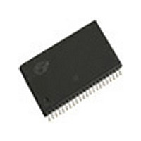
CY62127DV30LL-55ZI Cypress Semiconductor Corp, CY62127DV30LL-55ZI Datasheet - Page 3

CY62127DV30LL-55ZI
Manufacturer Part Number
CY62127DV30LL-55ZI
Description
Manufacturer
Cypress Semiconductor Corp
Datasheet
1.CY62127DV30LL-55ZI.pdf
(11 pages)
Specifications of CY62127DV30LL-55ZI
Density
1Mb
Access Time (max)
55ns
Sync/async
Asynchronous
Architecture
Not Required
Clock Freq (max)
Not RequiredMHz
Operating Supply Voltage (typ)
2.5/3.3V
Address Bus
16b
Package Type
TSOP-II
Operating Temp Range
-40C to 85C
Number Of Ports
1
Supply Current
10mA
Operating Supply Voltage (min)
2.2V
Operating Supply Voltage (max)
3.6V
Operating Temperature Classification
Industrial
Mounting
Surface Mount
Pin Count
44
Word Size
16b
Number Of Words
64K
Lead Free Status / Rohs Status
Not Compliant
Available stocks
Company
Part Number
Manufacturer
Quantity
Price
Company:
Part Number:
CY62127DV30LL-55ZI
Manufacturer:
CY
Quantity:
30 534
Document #: 38-05229 Rev. *H
Maximum Ratings
(Above which the useful life may be impaired. For user guide-
lines, not tested.)
Storage Temperature .................................. –65°C to +150°C
Ambient Temperature with
Power Applied............................................. –55°C to +125°C
Supply Voltage to Ground Potential
DC Voltage Applied to Outputs
in High-Z State
DC Electrical Characteristics
Capacitance
......................................................................... −0.3V to 3.9V
V
V
V
V
I
I
I
I
I
Parameter
Notes:
IX
OZ
CC
SB1
SB2
5. V
6. Full device operation requires linear ramp of V
7. Tested initially and after any design or proces changes that may affect these parameters.
OH
OL
IH
IL
IL(min.)
= −2.0V for pulse durations less than 20 ns., V
Parameter
Output HIGH
Voltage
Output LOW
Voltage
Input HIGH
Voltage
Input LOW
Voltage
Input Leakage
Current
Output
Leakage
Current
V
Supply Current
Automatic CE
Power-down
Current—
CMOS Inputs
Automatic CE
Power-down
Current—
CMOS Inputs
C
Description
CC
C
OUT
[5]
IN
[7]
....................................−0.3V to V
Operating
2.2 < V
2.7 < V
2.2 < V
2.7 < V
2.2 < V
2.7 < V
2.2 < V
2.7 < V
GND < V
GND < V
Disabled
f = f
f = 1 MHz
CE > V
V
< 0.2V,
f = f
Data Only),
f = 0 (OE, WE, BHE
and BLE)
CE > V
V
V
f = 0, V
IN
IN
IN
MAX
MAX
> V
> V
< 0.2V,
CC
CC
CC
CC
CC
CC
CC
CC
CC
CC
CC
CC
Test Conditions
CC
(Address and
= 1/t
Output Capacitance
I
O
Input Capacitance
(Over the Operating Range)
< V
< 2.7 I
< 3.6 I
< 2.7 I
< 3.6 I
< 2.7
< 3.6
< 2.7
< 3.6
− 0.2V,
− 0.2V,
= 3.6V
− 0.2V, V
− 0.2V or
CC
< V
Description
RC
from 0V to V
CC
CC
V
I
CMOS level
, Output
IH(max.)
OH
OH
OL
OL
OUT
CC
IN
= 0.1 mA
= 2.1 mA
= −0.1 mA 2.0
= −1.0 mA 2.4
= 3.6V,
CC
= 0 mA,
LL
LL
CC(min)
= Vcc+0.75V for pulse durations less than 20 ns.
L Ind’l
L Ind’l
+ 0.3V
Auto
Auto
Auto
Auto
Ind’l
Ind’l
& V
CC
Min. Typ.
−0.3
−0.3
1.8
2.2
−1
−1
must be stable at V
DC Input Voltage
Output Current into Outputs (LOW)............................. 20 mA
Static Discharge Voltage.......................................... > 2001V
(per MIL-STD-883, Method 3015)
Latch-up Current..................................................... > 200 mA
Operating Range
Automotive
Industrial
0.85
T
Range
6.5
1.5
1.5
1.5
1.5
–45
A
Test Conditions
= 25°C, f = 1 MHz
[4]
V
CC
Max. Min. Typ.
+ 0.3
+ 0.3
V
V
0.4
0.4
0.6
0.8
1.5
+1
+1
13
= V
CC
CC
5
4
5
4
CC(min)
CC(typ)
Ambient Temperature (T
−0.3
−0.3
2.0
2.4
1.8
2.2
−1
−4
−1
−4
[5]
for 500 µs.
................................ −0.3V to V
–40°C to +125°C
–40°C to +85°C
0.85
1.5
1.5
1.5
1.5
1.5
1.5
–55
5
[4]
Max. Min Typ.
+ 0.3
+ 0.3
V
V
0.4
0.4
0.6 −0.3
0.8 −0.3
1.5
+1
+4
+1
+4
10
15
15
CC
CC
5
4
5
4
Max.
CY62127DV30
8
8
2.0
2.4
1.8
2.2
−1
−1
A
)
0.85
1.5
1.5
1.5
1.5
–70
5
[4]
2.2V to 3.6V
2.2V to 3.6V
Page 3 of 11
V
+ 0.3
+ 0.3
Max.
V
V
0.4
0.4
0.6
0.8
1.5
CC
Unit
+1
+1
10
CC
5
4
5
4
CC
CC
pF
pF
[6]
+ 0.3V
Unit
mA
µA
µA
µA
µA
µA
µA
V
V
V
V
[+] Feedback


