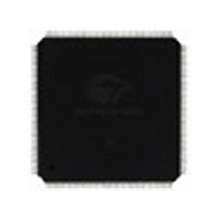
CY7C09579V-67AC Cypress Semiconductor Corp, CY7C09579V-67AC Datasheet - Page 17

CY7C09579V-67AC
Manufacturer Part Number
CY7C09579V-67AC
Description
Manufacturer
Cypress Semiconductor Corp
Datasheet
1.CY7C09579V-67AC.pdf
(32 pages)
Specifications of CY7C09579V-67AC
Density
1.125Mb
Access Time (max)
8ns
Sync/async
Synchronous
Architecture
SDR
Clock Freq (max)
40MHz
Operating Supply Voltage (typ)
3.3V
Address Bus
15b
Package Type
TQFP
Operating Temp Range
0C to 70C
Number Of Ports
2
Supply Current
340mA
Operating Supply Voltage (min)
3.135V
Operating Supply Voltage (max)
3.465V
Operating Temperature Classification
Commercial
Mounting
Surface Mount
Pin Count
144
Word Size
36b
Number Of Words
32K
Lead Free Status / Rohs Status
Not Compliant
Available stocks
Company
Part Number
Manufacturer
Quantity
Price
Part Number:
CY7C09579V-67AC
Manufacturer:
CYPRESS/赛普拉斯
Quantity:
20 000
Switching Waveforms
Flow-Through Read-to-Write-to-Read (OE = V
Flow-Through Read-to-Write-to-Read (OE Controlled)
Notes
Document Number: 38-06054 Rev. *D
42. ADS = V
43. Addresses do not have to be accessed sequentially since ADS = V
44. Timing shown is for x18 bus matching; x9 bus matching is similar with 4 cycles between address inputs.
45. See table “Right Port Operation“ for data output on first and subsequent cycles.
46. CE = ADS = CNTEN = V
47. During “No Operation,” data in memory at the selected address may be corrupted and should be rewritten to ensure data integrity.
48. Output state (HIGH, LOW, or High-Impedance) is determined by the previous cycle control signals.
ADDRESS
ADDRESS
DATA
DATA
DATA
DATA
CLK
R/W
OUT
CLK
R/W
OE
OUT
CE
CE
IN
IN
IL
, CNTEN = V
t
t
t
t
SW
SW
SA
SA
IL
IL
A
and CNTRST = V
A
; CNTRST = V
n
n
t
t
t
t
CD1
CD1
CH1
CH1
t
t
CYC1
CYC1
t
t
t
t
(continued)
HW
HW
HA
HA
t
t
CL1
CL1
IH
Q
.
IH
n
t
Q
DC
.
n
A
A
n+1
n+1
READ
READ
t
DC
t
CD1
t
t
SW
SD
t
OHZ
IL
t
CKHZ
IL
)
Q
[42, 43, 44, 45, 46, 47]
constantly loads the address on the rising edge of the CLK. Numbers are for reference only.
A
n+1
A
D
n+2
n+2
n+2
OPERATION
[42 , 43, 46, 47, 48]
NO
t
t
HW
HD
t
t
SW
SD
WRITE
A
D
A
D
n+2
n+2
n+3
n+3
WRITE
t
t
HW
HD
A
A
n+4
n+3
t
OE
t
t
CKLZ
t
CKLZ
t
CD1
CD1
READ
READ
Q
t
Q
t
DC
DC
CY7C09569V
CY7C09579V
n+3
A
n+4
A
n+4
n+5
t
t
CD1
CD1
Page 17 of 32
[+] Feedback


