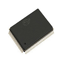
CY7C1360B-200AC Cypress Semiconductor Corp, CY7C1360B-200AC Datasheet - Page 24

CY7C1360B-200AC
Manufacturer Part Number
CY7C1360B-200AC
Description
Manufacturer
Cypress Semiconductor Corp
Datasheet
1.CY7C1360B-200AC.pdf
(34 pages)
Specifications of CY7C1360B-200AC
Density
9Mb
Access Time (max)
3ns
Sync/async
Synchronous
Architecture
SDR
Clock Freq (max)
200MHz
Operating Supply Voltage (typ)
3.3V
Address Bus
18b
Package Type
TQFP
Operating Temp Range
0C to 70C
Number Of Ports
1
Supply Current
220mA
Operating Supply Voltage (min)
3.135V
Operating Supply Voltage (max)
3.465V
Operating Temperature Classification
Commercial
Mounting
Surface Mount
Pin Count
100
Word Size
36b
Number Of Words
256K
Lead Free Status / Rohs Status
Not Compliant
Document #: 38-05291 Rev. *C
AC Test Loads and Waveforms
Note:
Capacitance
15. Tested initially and after any design or process change that may affect these parameters.
Thermal Resistance
C
C
C
IN
CLK
I/O
OUTPUT
OUTPUT
Parameter
Parameter
3.3V I/O Test Load
2.5V I/O Test Load
Θ
Θ
JA
JC
Z
Z
[15]
0
0
Thermal Resistance
(Junction to Ambient)
Thermal Resistance
(Junction to Case)
Input Capacitance
Clock Input Capacitance
Input/Output Capacitance
= 50Ω
= 50Ω
Description
(a)
(a)
V
Description
V
[15]
L
L
= 1.25V
= 1.5V
R
R
L
L
= 50Ω
= 50Ω
OUTPUT
OUTPUT
3.3V
2.5V
Test conditions follow standard
test methods and procedures
for measuring thermal
impedance, per EIA / JESD51.
INCLUDING
INCLUDING
T
V
V
A
DD
DDQ
JIG AND
JIG AND
SCOPE
SCOPE
= 25°C, f = 1 MHz,
Test Conditions
5 pF
5 pF
= 3.3V.
Test Conditions
= 2.5V
(b)
(b)
R = 317Ω
R = 1667Ω
R = 351Ω
R =1538Ω
Package
V
Package
TQFP
GND
GND
DD
TQFP
V
5
5
5
DD
25
9
≤ 1 ns
≤ 1 ns
10%
10%
Package
Package
BGA
ALL INPUT PULSES
ALL INPUT PULSES
BGA
5
5
7
25
6
90%
90%
(c)
(c)
Package
CY7C1360B
CY7C1362B
Package
fBGA
fBGA
5
5
7
27
6
Page 24 of 34
90%
90%
10%
10%
°C/W
°C/W
≤ 1 ns
≤ 1 ns
Unit
Unit
pF
pF
pF


