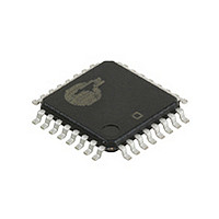
CY2HH8110AC Cypress Semiconductor Corp, CY2HH8110AC Datasheet - Page 3

CY2HH8110AC
Manufacturer Part Number
CY2HH8110AC
Description
Manufacturer
Cypress Semiconductor Corp
Datasheet
1.CY2HH8110AC.pdf
(7 pages)
Specifications of CY2HH8110AC
Number Of Outputs
10
Operating Supply Voltage (max)
1.65V
Operating Temp Range
0C to 85C
Propagation Delay Time
7ns
Operating Supply Voltage (min)
1.38V
Mounting
Surface Mount
Pin Count
32
Operating Supply Voltage (typ)
1.5V
Package Type
TQFP
Quiescent Current
1mA
Input Frequency
150MHz
Duty Cycle
55%
Operating Temperature Classification
Commercial
Lead Free Status / Rohs Status
Not Compliant
Available stocks
Company
Part Number
Manufacturer
Quantity
Price
Company:
Part Number:
CY2HH8110AC
Manufacturer:
CY
Quantity:
24
Document #: 38-07556 Rev **
Absolute Maximum Conditions
DC Electrical Specifications
AC Electrical Specifications
Multiple Supplies: The voltage on any input or I/O pin cannot exceed the power pin during power-up. Power supply sequencing is NOT required.
f
V
V
t
DC
Notes:
in
r
3.
4.
5.
6.
IL
IH
Parameter
, t
Parameter
Parameter
(AC)
(AC)
f
Driving 50 series terminated or symmetrically double parallel terminated transmission line to a termination voltage of V
Inputs have pull-down resistors that affect the input current.
AC characteristics apply for series or parallel output termination to V
tr/tf times are faster with parallel terminated loads.
ESD
V
V
V
C
R
Ø
Ø
Z
V
I
V
FIT
LU
V
T
V
OUT
T
T
DDQ
C
V
V
V
V
I
I
OUT
DD
DD
I
OUT
TT
PS
DD
IN
JC
JA
A
OH
IH
S
OL
IL
J
IH
IH
IN
IL
IL
H
DC Supply Voltage
DC Operating Voltage
DC Input Voltage
DC Output Voltage
Output termination Voltage
Latch Up Immunity
Power Supply Ripple
Temperature, Storage
Temperature, Operating Ambient
Temperature, Junction
Dissipation, Junction to Case
Dissipation, Junction to Ambient
ESD Protection (Human Body
Model)
Failure in Time
Input Frequency
AC Input HIGH Voltage
AC Input LOW Voltage
Output rise/fall time
Output duty cycle
Input Voltage, Low
Input Voltage, High
Input Voltage, Low
Input Voltage, High
Output Voltage, Low
Output Voltage, High
Input Current, Low
Input Current, High
Quiescent Supply Current
Dynamic Supply Current
Input Pin Capacitance
Output Pin Capacitance
Output Impedance
Description
Description
Description
[4]
[6]
[4]
(V
(V
[3]
[3]
DD
DD
= 1.5V ± 8%, T
= 1.5V ± 8%, T
Reference
20% to 80%
Fout > 100 MHz
V
Fout < 100 MHz
HSTL input, V
OE# input
I
I
V
V
V
Outputs loaded @ 62.5 MHz
OL
OH
Functional
Relative to V
applied
Relative to V
Functional
Ripple Frequency < 100 kHz
Non-functional
Functional
Functional
Functional
Functional
Manufacturing test
REF
IL
IH
IN
= 16 mA
= V
= –16 mA
= V
= 0V, outputs disabled
A
A
TT
=V
. Parameters are guaranteed by characterization and are not 100% tested.
= 0°C to +85°C)
= 0°C to +85°C)
SS
DD
DD
Condition
Condition
Condition
/2, Internal Voltage
SS
SS
REF
, with or V
= 0.75V
[5]
DD
0.7 * V
–0.30
-0.30
Min.
0.95
Min.
0.85
-0.3
0.3
1.0
48
45
–
–
1600
–
–
–
–
–
–
–
Min.
–0.5
1.35
–0.5
-0.5
200
–65
0
DD
Typ.
Typ.
215
10
4.5
25
–
–
–
–
–
–
TT
–
–
–
–
–
–
–
–
–
–
.
V
V
V
DD
DD
Max.
DD
+150
+150
1.65
+85
150
105
2.5
42
V
V
0.3 * V
CY2HH8110
+ 0.5
+ 0.5
DD
DD
Max.
Max.
0.55
0.65
1.80
150
–10
100
250
1.5
0.4
52
55
2
1
6
6
–
+ 0.3
+ 0.3
DD
Page 3 of 7
mVp-p
°C/W
°C/W
Unit
ppm
mA
Unit
MHz
°C
°C
°C
Unit
V
V
V
V
V
V
mA
mA
pF
pF
ns
%
V
V
V
V
V
V
V
V
A
A
[+] Feedback


