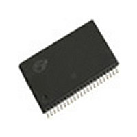
CY62146VLL-70ZI Cypress Semiconductor Corp, CY62146VLL-70ZI Datasheet - Page 4

CY62146VLL-70ZI
Manufacturer Part Number
CY62146VLL-70ZI
Description
Manufacturer
Cypress Semiconductor Corp
Datasheet
1.CY62146VLL-70ZI.pdf
(10 pages)
Specifications of CY62146VLL-70ZI
Density
4Mb
Access Time (max)
70ns
Sync/async
Asynchronous
Architecture
Not Required
Clock Freq (max)
Not RequiredMHz
Operating Supply Voltage (typ)
3V
Address Bus
18b
Package Type
TSOP-II
Operating Temp Range
-40C to 85C
Number Of Ports
1
Supply Current
15mA
Operating Supply Voltage (min)
2.7V
Operating Supply Voltage (max)
3.6V
Operating Temperature Classification
Industrial
Mounting
Surface Mount
Pin Count
44
Word Size
16b
Number Of Words
256K
Lead Free Status / Rohs Status
Not Compliant
Available stocks
Company
Part Number
Manufacturer
Quantity
Price
Company:
Part Number:
CY62146VLL-70ZI
Manufacturer:
CYPRESS
Quantity:
14
Company:
Part Number:
CY62146VLL-70ZIT
Manufacturer:
LATTICE
Quantity:
5
Document #: 38-05159 Rev. *A
Data Retention Characteristics
Data Retention Waveform
Switching Characteristics
V
I
t
t
Read Cycle
t
t
t
t
t
t
t
t
t
t
t
t
t
t
Write Cycle
t
Notes:
10. The minimum write cycle time for Write Cycle #3 (WE controlled, OE LOW) is the sum of t
Parameter
CCDR
CDR
R
RC
AA
OHA
ACE
DOE
LZOE
HZOE
LZCE
HZCE
PU
PD
DBE
LZBE
HZBE
WC
5.
6.
7.
8.
9.
DR
[5]
Full Device AC operation requires linear V
Test conditions assume signal transition time of 5 ns or less, timing reference levels of 1.5V, input pulse levels of 0 to V
I
At any given temperature and voltage condition, t
t
The internal write time of the memory is defined by the overlap of CE LOW and WE LOW. Both signals must be LOW to initiate a write and either signal can
terminate a write by going HIGH. The data input set-up and hold timing should be referenced to the rising edge of the signal that terminates the write.
[4]
OL
HZOE
/I
OH
V
, t
CE
CC
and 30 pF load capacitance.
HZCE
[9, 10]
Parameter
Parameter
V
Data Retention Current
Chip Deselect to Data
Retention Time
Operation Recovery Time
, and t
CC
R
V
R1
R2
for Data Retention)
TH
TH
HZWE
Description
are specified with C
Over the Operating Range
CC
Read Cycle Time
Address to Data Valid
Data Hold from Address Change
CE LOW to Data Valid
OE LOW to Data Valid
OE LOW to Low-Z
OE HIGH to High-Z
CE LOW to Low-Z
CE HIGH to High-Z
CE LOW to Power-up
CE HIGH to Power-down
BHE / BLE LOW to Data Valid
BHE / BLE LOW to Low-Z
BHE / BLE HIGH to High-Z
Write Cycle Time
L
ramp from V
= 5 pF as in part (b) of AC Test Loads. Transition is measured 500 mV from steady-state voltage.
V
(Over the Operating Range)
CC(min.)
t
CDR
HZCE
V
0.3V; No input may exceed V
CC
= 1.0V, CE > V
is less than t
DR
to V
CC(min.)
[7]
[7, 8]
LZCE
[7, 8]
[8]
DATA RETENTION MODE
1550
3.0V
1105
1.75
645
CC
, t
> 10 s or stable V
HZOE
[6]
Description
Conditions
– 0.3V, V
is less than t
V
DR
> 1.0 V
IN
CC
> V
HZWE
+ 0.3V
CC(min.)
LZOE
CC
and t
, and t
– 0.3V or V
>10 s.
SD
HZWE
.
is less than t
IN
<
CC(typ.)
V
CC(min.)
CY62146V MoBL
Min. Typ.
t
1.0
70
R
0
, and output loading of the specified
LZWE
Min.
Ohms
Ohms
Ohms
for any given device.
70
10
10
70
Unit
5
0
5
V
1
70 ns
[3]
Max.
3.6
Max.
10
Page 4 of 10
70
70
25
20
20
70
35
20
Unit
ns
ns
Unit
V
A
ns
ns
ns
ns
ns
ns
ns
ns
ns
ns
ns
ns
ns
ns
ns
®
[+] Feedback


