MTB33N10E ON Semiconductor, MTB33N10E Datasheet - Page 2
MTB33N10E
Manufacturer Part Number
MTB33N10E
Description
Manufacturer
ON Semiconductor
Type
Power MOSFETr
Datasheet
1.MTB33N10E.pdf
(10 pages)
Specifications of MTB33N10E
Number Of Elements
1
Polarity
N
Channel Mode
Enhancement
Drain-source On-res
0.06Ohm
Drain-source On-volt
100V
Gate-source Voltage (max)
±20V
Continuous Drain Current
33A
Power Dissipation
2.5W
Operating Temp Range
-55C to 150C
Operating Temperature Classification
Military
Mounting
Surface Mount
Pin Count
2 +Tab
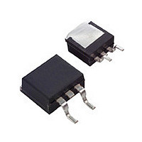
Package Type
D2PAK
Dc
0106
Lead Free Status / Rohs Status
Not Compliant
Available stocks
Company
Part Number
Manufacturer
Quantity
Price
Company:

Part Number:
MTB33N10E
Manufacturer:
ON
Quantity:
1 537


1. Pulse Test: Pulse Width ≤ 300 μs, Duty Cycle ≤ 2%.
2. Switching characteristics are independent of operating junction temperature.
OFF CHARACTERISTICS
ON CHARACTERISTICS (Note 1)
DYNAMIC CHARACTERISTICS
SWITCHING CHARACTERISTICS (Note 2)
SOURCE−DRAIN DIODE CHARACTERISTICS
INTERNAL PACKAGE INDUCTANCE
ELECTRICAL CHARACTERISTICS
Drain−Source Breakdown Voltage
Zero Gate Voltage Drain Current
Gate−Body Leakage Current (V
Gate Threshold Voltage
Static Drain−Source On−Resistance (V
Drain−Source On−Voltage (V
Forward Transconductance (V
Input Capacitance
Output Capacitance
Reverse Transfer Capacitance
Turn−On Delay Time
Rise Time
Turn−Off Delay Time
Fall Time
Gate Charge
Forward On−Voltage (Note 1)
Reverse Recovery Time
Reverse Recovery Stored Charge
Internal Drain Inductance
Internal Source Inductance
(V
Temperature Coefficient (Positive)
(V
(V
(V
Temperature Coefficient (Negative)
(I
(I
(See Figure 8)
(See Figure 14)
(Measured from the drain lead 0.25″ from package to center of die)
(Measured from the source lead 0.25″ from package to source bond pad)
D
D
GS
DS
DS
DS
= 33 Adc)
= 16.5 Adc, T
= 0 Vdc, I
= 100 Vdc, V
= 100 Vdc, V
= V
GS
, I
D
D
= 250 μAdc)
J
= 250 μAdc)
= − 25°C)
GS
GS
= 0 Vdc)
= 0 Vdc, T
GS
Characteristic
DS
GS
= 10 Vdc)
= 8.0 Vdc, I
J
= ± 20 Vdc, V
= − 25°C)
GS
(T
(V
(V
= 10 Vdc, I
(V
J
(I
(I
(I
DS
DS
S
S
S
= 25°C unless otherwise noted)
DD
D
= 33 Adc, V
= 33 Adc, V
= 33 Adc, V
= 16.5 Adc)
= 25 Vdc, V
dI
= 80 Vdc, I
= 50 Vdc, I
DS
V
V
S
f = 1.0 MHz)
R
T
/dt = 100 A/μs)
GS
GS
= 0)
J
G
D
= 125°C)
= 10 Vdc,
= 10 Vdc)
= 9.1 Ω)
= 16.5 Adc)
http://onsemi.com
GS
GS
GS
D
D
GS
= 33 Adc,
= 33 Adc,
= 0 Vdc)
= 0 Vdc,
= 0 Vdc,
= 0 Vdc,
2
V
Symbol
R
V
V
(BR)DSS
t
t
I
C
I
DS(on)
DS(on)
Q
GS(th)
C
C
V
g
d(on)
d(off)
DSS
GSS
Q
Q
Q
Q
L
L
t
t
t
oss
t
t
FS
rss
SD
RR
iss
rr
a
b
r
f
D
S
T
1
2
3
Min
100
2.0
8.0
−
−
−
−
−
−
−
−
−
−
−
−
−
−
−
−
−
−
−
−
−
−
−
−
−
−
−
1830
0.04
0.98
0.93
Typ
118
678
559
164
144
108
7.0
1.6
1.0
4.5
7.5
18
48
83
52
12
32
24
36
−
−
−
−
−
−
−
2500
1200
1100
Max
0.06
100
100
330
100
170
110
4.0
2.4
2.1
2.0
10
40
−
−
−
−
−
−
−
−
−
−
−
−
−
−
mV/°C
mV/°C
μAdc
mhos
nAdc
Ohm
Unit
Vdc
Vdc
Vdc
Vdc
nC
μC
nH
nH
pF
ns
ns
Related parts for MTB33N10E
Image
Part Number
Description
Manufacturer
Datasheet
Request
R

Part Number:
Description:
ON Semiconductor [VOLTAGE REGULATOR]
Manufacturer:
ON Semiconductor
Datasheet:
Part Number:
Description:
357-036-542-201 CARDEDGE 36POS DL .156 BLK LOPRO
Manufacturer:
ON Semiconductor
Datasheet:
Part Number:
Description:
357-036-542-201 CARDEDGE 36POS DL .156 BLK LOPRO
Manufacturer:
ON Semiconductor
Datasheet:
Part Number:
Description:
357-036-542-201 CARDEDGE 36POS DL .156 BLK LOPRO
Manufacturer:
ON Semiconductor
Datasheet:
Part Number:
Description:
357-036-542-201 CARDEDGE 36POS DL .156 BLK LOPRO
Manufacturer:
ON Semiconductor
Datasheet:
Part Number:
Description:
357-036-542-201 CARDEDGE 36POS DL .156 BLK LOPRO
Manufacturer:
ON Semiconductor
Datasheet:
Part Number:
Description:
357-036-542-201 CARDEDGE 36POS DL .156 BLK LOPRO
Manufacturer:
ON Semiconductor
Datasheet:
Part Number:
Description:
357-036-542-201 CARDEDGE 36POS DL .156 BLK LOPRO
Manufacturer:
ON Semiconductor
Datasheet:
Part Number:
Description:
357-036-542-201 CARDEDGE 36POS DL .156 BLK LOPRO
Manufacturer:
ON Semiconductor
Datasheet:
Part Number:
Description:
357-036-542-201 CARDEDGE 36POS DL .156 BLK LOPRO
Manufacturer:
ON Semiconductor
Datasheet:
Part Number:
Description:
357-036-542-201 CARDEDGE 36POS DL .156 BLK LOPRO
Manufacturer:
ON Semiconductor
Datasheet:
Part Number:
Description:
Manufacturer:
ON Semiconductor
Datasheet:
Part Number:
Description:
Manufacturer:
ON Semiconductor
Datasheet:
Part Number:
Description:
Manufacturer:
ON Semiconductor
Datasheet: