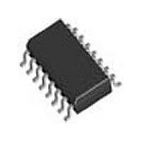
LTC1235CS Linear Technology, LTC1235CS Datasheet - Page 12

LTC1235CS
Manufacturer Part Number
LTC1235CS
Description
Manufacturer
Linear Technology
Datasheet
1.LTC1235CS.pdf
(16 pages)
Specifications of LTC1235CS
Number Of Elements
1
Monitored Voltage 1 (typ)
4.65V
Battery Backup Switching
Yes
Watchdog Timer
Yes
Chip Enable Signals
Yes
Reset Active Time
280ms
Manual Reset
Yes
Package Type
SOL
Operating Supply Voltage (min)
4.75V
Operating Supply Voltage (max)
5.5V
Reset Threshold Voltage (max)
4.75V
Reset Threshold Voltage (min)
4.5V
Power Dissipation
500mW
Operating Temp Range
0C to 70C
Operating Temperature Classification
Commercial
Power Fail Detection
Yes
Mounting
Surface Mount
Pin Count
16
Supply Current
1.5mA
Lead Free Status / Rohs Status
Not Compliant
Available stocks
Company
Part Number
Manufacturer
Quantity
Price
Part Number:
LTC1235CS
Manufacturer:
LINEAR/凌特
Quantity:
20 000
Part Number:
LTC1235CS#TRPBF
Manufacturer:
LTNEAR
Quantity:
20 000
Part Number:
LTC1235CSW
Manufacturer:
LINEAR/凌特
Quantity:
20 000
Part Number:
LTC1235CSW#PBF
Manufacturer:
LINEAR/凌特
Quantity:
20 000
Part Number:
LTC1235CSW#TR
Manufacturer:
LT/凌特
Quantity:
20 000
APPLICATIONS INFORMATION
LTC1235
Power Fail Warning
The LTC1235 generates a Power Failure Output (PFO) for
early warning of failure in the microprocessor’s power sup-
ply. This is accomplished by comparing the Power Failure
Input (PFI) with an internal 1.3V reference. PFO goes low
when the voltage at PFI pin is less than 1.3V. Typically
PFI is driven by an external voltage divider (R1 and R2 in
Figures 8 and 9) which senses either an unregulated DC
input or a regulated 5V output. The voltage divider ratio can
be chosen such that the voltage at PFI pin falls below 1.3V
several milliseconds before the +5V supply falls below the
maximum reset voltage threshold 4.75V. PFO is normally
used to interrupt the microprocessor to execute shutdown
procedure between PFO and RESET or RESET.
The power fail comparator, C3, does not have hysteresis.
Hysteresis can be added however, by connecting a resistor
between the PFO output and the noninverting PFI input
pin as shown in Figures 8 and 9. The upper and lower trip
points in the comparator are established as follows:
When PFO output is low, R3 sinks current from the sum-
ming junction at the PFI pin.
When PFO output is high, the series combination of R3
and R4 source current into the PFI summing junction.
Example 1: The circuit in Figure 8 demonstrates the use
of the power fail comparator to monitor the unregulated
power supply input. Assuming the rate of decay of the
supply input V
a shut-down procedure is 8ms. Also the noise of V
200mV. With these assumptions in mind, we can reason-
ably set V
maximum reset voltage threshold and the dropout voltage
of LT1086-5 (4.75V + 1.5V) and V
12
V
V
Assuming R4«R3,V
H
L
=1.3V 1+
= 1.3V 1+
L
= 7.5V which 1.25V greater than the sum of
IN
is 100mV/ms and the total time to execute
R2
R2
R1
R1
+
±
R3
1.3V(R3+R4)
R1
(5V ± 1.3V)R1
HYST
= 5V
HYST
R3
R1
= 850mV.
IN
is
Choose R3 = 300k and R1 = 51k. Also select R4 = 10k
which is much smaller than R3.
R2 = 9.7k, Choose nearest 5% resistor 10k and recalculate
V
L
V
+
IN
,
V
R3 ≈ 5.88 R1
V
7.5V = 1.3V 1+
V
V
V
(7.32V – 6.25V)
IN
≥ 6.5V
HYST
HYST
H
10μF
L
≥ 7.5V
R1
51k
R2
10k
Figure 8. Monitoring Unregulated DC Supply with the
LTC1235 Power Fail Comparator
10μF
Figure 9. Monitoring Regulated DC Supply with the
LTC1235 Power Fail Comparator
100mV/ms
=1.3V 1+
=1.3V 1+
+
= 8.151V – 7.32V = 831mV
V
= 5V
LT1086-5
IN
ADJ
V
V
LT1086-5
IN
OUT
ADJ
R3
R1
V
OUT
10μF
10k
51k
10k
51k
= 850mV
+
51k
R2
=
+
+
±
10.7ms
100μF
(5V ± 1.3V)51k
300k
R1
27k
R2
8.2k
R5
3.3k
300k
±
51k
R3
1.3V(310k)
(5V ± 1.3V)51k
2.7M
1.3V(310k)
+5V
R3
10k
R4
+5V
R4
10k
0.1μF
= 8.151V
0.1μF
PFI
V
PFO
PFI
PFO
V
CC
= 7.32V
CC
LTC1235
LTC1235
GND
BACKUP
GND
BACKUP
TO μP
TO μP
1235 F08
1235 F09
1235fa


