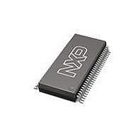
74LVT16652ADL NXP Semiconductors, 74LVT16652ADL Datasheet

74LVT16652ADL
Specifications of 74LVT16652ADL
Available stocks
Related parts for 74LVT16652ADL
74LVT16652ADL Summary of contents
Page 1
V 16-bit bus transceiver/register; 3-state Rev. 03 — 12 January 2005 1. General description The 74LVT16652A is a high-performance BiCMOS product designed for V 3.3 V. The device can be used as two 8-bit transceivers or one 16-bit ...
Page 2
... PLH t PHL I Ordering information Table 2: Ordering information Type number Package Temperature range Name 74LVT16652ADGG +85 C 74LVT16652ADL +85 C 9397 750 14402 Product data sheet Quick reference data Conditions propagation delay pF nAx to nBx or nBx to nAx propagation delay pF nAx to nBx or nBx to nAx input capacitance ...
Page 3
Philips Semiconductors 5. Functional diagram Fig 1. Logic symbol Fig 2. IEC Logic symbol 9397 750 14402 Product data sheet 3.3 V 16-bit bus transceiver/register; 3-state 1A0 1A1 1A2 1A3 2 1CPAB 3 1SAB 55 1CPBA ...
Page 4
Philips Semiconductors Fig 3. Logic diagram 9397 750 14402 Product data sheet nOEBA nOEAB nCPBA nSBA nCPAB nSAB CHANNELS nA0 nA1 nA2 nA3 nA4 nA5 nA6 nA7 Rev. 03 — 12 January 2005 74LVT16652A ...
Page 5
Philips Semiconductors 6. Pinning information 6.1 Pinning Fig 4. Pin configuration 6.2 Pin description Table 3: Symbol 1OEAB 1CPAB 1SAB GND 1A0 1A1 V CC 1A2 9397 750 14402 Product data sheet 1 1OEAB 1CPAB 2 1SAB 3 4 GND ...
Page 6
Philips Semiconductors Table 3: Symbol 1A3 1A4 GND 1A5 1A6 1A7 2A0 2A1 2A2 GND 2A3 2A4 2A5 V CC 2A6 2A7 GND 2SAB 2CPAB 2OEAB 2OEBA 2CPBA 2SBA GND 2B7 2B6 V CC 2B5 2B4 2B3 GND 2B2 2B1 ...
Page 7
Philips Semiconductors Table 3: Symbol V CC 1B1 1B0 GND 1SBA 1CPBA 1OEBA 7. Functional description 7.1 Function table [1] Table 4: Function table Operating mode Input nOEAB nOEBA nCPAB Isolation L Store A and B data L Store A, ...
Page 8
Philips Semiconductors 7.2 Bus management function Figure 5 performed with the 74LVT16652A. The select pins determine whether data is stored or transferred through the device in real time. The output enable pins determine the direction of the data flow. A ...
Page 9
Philips Semiconductors 8. Limiting values Table 5: In accordance with the Absolute Maximum Rating System (IEC 60134). Voltages are referenced to GND (ground = 0 V). Symbol ...
Page 10
Philips Semiconductors 10. Static characteristics Table 7: Static characteristics At recommended operating conditions; voltages are referenced to GND (ground = 0 V). Symbol Parameter [ +85 C amb V input clamp voltage IK V HIGH-level ...
Page 11
Philips Semiconductors Table 7: Static characteristics At recommended operating conditions; voltages are referenced to GND (ground = 0 V). Symbol Parameter I additional supply current CC per input pin C input capacitance control I pins C I/O pin capacitance I/O ...
Page 12
Philips Semiconductors Table 8: Dynamic characteristics GND = 2 Symbol Parameter t propagation delay PHL nAx to nBx or nBx to nAx propagation delay nCPAB ...
Page 13
Philips Semiconductors Table 9: Dynamic characteristics setup requirements GND = 2 Symbol Parameter [ +85 C amb t set-up time ...
Page 14
Philips Semiconductors Fig 7. Propagation delay nAx to nBx or nBx to nAx Fig 8. Propagation delay SBA to nAx or SAB to nBx Fig 9. 3-state output enable time to HIGH-level and output disable time from HIGH-level 9397 750 ...
Page 15
Philips Semiconductors Fig 10. 3-state output enable time to LOW-level and output disable time from LOW-level Fig 11. Data set-up and hold times 9397 750 14402 Product data sheet nOEBA V M nOEAB t PZL nAx or nBx V is ...
Page 16
Philips Semiconductors a. Input pulse definition b. Test circuit Fig 12. Load circuitry for switching times Table 10: Input V I 2.7 V 9397 750 14402 Product data sheet negative V M pulse ...
Page 17
Philips Semiconductors 13. Package outline TSSOP56: plastic thin shrink small outline package; 56 leads; body width 6 pin 1 index 1 DIMENSIONS (mm are the original dimensions). A UNIT max. ...
Page 18
Philips Semiconductors SSOP56: plastic shrink small outline package; 56 leads; body width 7 pin 1 index 1 e DIMENSIONS (mm are the original dimensions) A UNIT max. 0.4 2.35 mm ...
Page 19
Philips Semiconductors 14. Revision history Table 11: Revision history Document ID Release date 74LVT16652A_3 20050112 • Modifications: The format of this data sheet has been redesigned to comply with the new presentation and information standard of Philips Semiconductors. • Product ...
Page 20
Philips Semiconductors 15. Data sheet status [1] Level Data sheet status Product status I Objective data Development II Preliminary data Qualification III Product data Production [1] Please consult the most recently issued data sheet before initiating or completing a design. ...
Page 21
Philips Semiconductors 19. Contents 1 General description . . . . . . . . . . . . . . . . . . . . . . 1 2 Features . . . . . . . . ...


