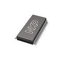
74LVT16652ADL NXP Semiconductors, 74LVT16652ADL Datasheet - Page 11

74LVT16652ADL
Manufacturer Part Number
74LVT16652ADL
Description
Bus Transceivers 3.3V 16-BIT BUS XCVR 3-S
Manufacturer
NXP Semiconductors
Datasheet
1.74LVT16652ADL.pdf
(21 pages)
Specifications of 74LVT16652ADL
Logic Type
BiCMOS
Logic Family
LVT
Number Of Channels Per Chip
16
Input Level
LVTTL
Output Level
LVTTL
Output Type
3-State
High Level Output Current
- 32 mA
Low Level Output Current
64 mA
Propagation Delay Time
2.7 ns
Supply Voltage (max)
3.6 V
Supply Voltage (min)
2.7 V
Maximum Operating Temperature
+ 85 C
Package / Case
SSOP-56
Function
Bus Transceiver / Register
Minimum Operating Temperature
- 40 C
Mounting Style
SMD/SMT
Number Of Circuits
2
Polarity
Non-Inverting
Lead Free Status / Rohs Status
Details
Other names
74LVT16652ADL,512
Available stocks
Company
Part Number
Manufacturer
Quantity
Price
Company:
Part Number:
74LVT16652ADL
Manufacturer:
MAXIM
Quantity:
1 400
Philips Semiconductors
Table 7:
At recommended operating conditions; voltages are referenced to GND (ground = 0 V).
[1]
[2]
[3]
[4]
[5]
[6]
[7]
[8]
11. Dynamic characteristics
Table 8:
GND = 0 V; t
9397 750 14402
Product data sheet
Symbol
C
C
Symbol
T
f
t
max
PLH
I
amb
I
I/O
CC
All typical values are measured at V
For valid test results, data must not be loaded into the flip-flops (or latches) after applying power.
Unused pins at V
This is the bus-hold overdrive current required to force the input to the opposite logic state.
This parameter is valid for any V
a transition time of 100 s is permitted. This parameter is valid for T
I
I
This is the increase in supply current for each input at the specified voltage level other than V
CC
CC
= 40 C to +85 C
is measured with 16 outputs LOW.
is measured with outputs pulled to V
Static characteristics
Dynamic characteristics
r
Parameter
additional supply current
per input pin
input capacitance control
pins
I/O pin capacitance
Parameter
maximum clock frequency
propagation delay
nAx to nBx or nBx to nAx
propagation delay
nCPAB to nBx or
nCPBA to nAx
propagation delay
nSAB to nBx or
nSBA to nAx
= t
f
= 2.5 ns; C
CC
or GND.
[1]
L
= 50 pF; R
CC
…continued
between 0 V and 1.2 V with a transition time of up to 10 ms. From V
CC
= 3.3 V and T
CC
Conditions
V
V
or GND
V
outputs disabled; V
3.0 V
L
CC
CC
I
= 500 ; test circuit see
or GND.
= 0 V or 3.0 V
Conditions
V
see
see
see
see
CC
= 3.3 V
V
V
V
V
V
V
CC
CC
CC
CC
CC
CC
0.6 V; other inputs at V
Figure 6
Figure 7
Figure 6
Figure 8
= 2.7 V or 3.3 V
Rev. 03 — 12 January 2005
= 3.3 V
= 2.7 V
= 3.3 V
= 2.7 V
= 3.3 V
= 2.7 V
amb
= 25 C.
0.3 V; one input at
0.3 V
0.3 V
0.3 V
I
= 0 V or
amb
0.3 V;
Figure
= 25 C only.
CC
3.3 V 16-bit bus transceiver/register; 3-state
12.
[8]
Min
-
-
-
Min
150
0.5
-
1.5
-
1.0
-
CC
or GND.
© Koninklijke Philips Electronics N.V. 2005. All rights reserved.
74LVT16652A
Typ
0.1
3
9
Typ
180
2.1
-
2.5
-
2.3
-
CC
= 1.2 V to V
Max
0.2
-
-
Max
-
3.4
3.9
4.2
4.7
4.5
5.4
CC
= 3.3 V
Unit
mA
pF
pF
Unit
MHz
ns
ns
ns
ns
ns
ns
11 of 21
0.3 V


