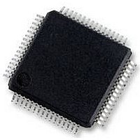
AD7609BSTZ Analog Devices Inc, AD7609BSTZ Datasheet - Page 23

AD7609BSTZ
Manufacturer Part Number
AD7609BSTZ
Description
58T8900
Manufacturer
Analog Devices Inc
Datasheet
1.AD7609BSTZ.pdf
(36 pages)
Specifications of AD7609BSTZ
Resolution (bits)
18bit
Sampling Rate
250kSPS
Input Channel Type
Differential
Data Interface
Serial, SPI
Supply Voltage Range - Analog
4.75V To 5.25V
Rohs Compliant
Yes
Available stocks
Company
Part Number
Manufacturer
Quantity
Price
Company:
Part Number:
AD7609BSTZ
Manufacturer:
ADI
Quantity:
433
Company:
Part Number:
AD7609BSTZ
Manufacturer:
ADI
Quantity:
250
Company:
Part Number:
AD7609BSTZ
Manufacturer:
Analog Devices Inc
Quantity:
10 000
Part Number:
AD7609BSTZ
Manufacturer:
ADI/亚德诺
Quantity:
20 000
Company:
Part Number:
AD7609BSTZ-RL
Manufacturer:
Analog Devices Inc
Quantity:
10 000
INTERNAL/EXTERNAL REFERENCE
The
REFIN/REFOUT pin allows access to the 2.5 V reference that
generates the on-chip 4.5 V reference internally, or it allows an
external reference of 2.5 V to be applied to the AD7609. An
externally applied reference of 2.5 V is also amplified to 4.5 V using
the internal buffer. This 4.5 V buffered reference is the reference
used by the SAR ADC.
The REF SELECT pin is a logic input pin that allows the user to
select between the internal reference and the external reference.
If this pin is set to logic high, the internal reference is selected
and is enabled; if this pin is set to logic low, the internal refer-
ence is disabled and an external reference voltage must be
applied to the REFIN/REFOUT pin. The internal reference
buffer is always enabled. After a reset, the
the reference mode selected by the REF SELECT pin. Decoupling
is required on the REFIN/REFOUT pin for both the internal
or external reference options. A 10 μF ceramic capacitor is
required on the REFIN/REFOUT to ground close to the
REFGND pins. The
configured to amplify the REF voltage up to ~4.5 V, as shown
in Figure 38. The REFCAPA and REFCAPB pins must be
shorted together externally and a ceramic capacitor of 10 μF
applied to REFGND to ensure the reference buffer is in
closed-loop operation. The reference voltage available at the
REFIN/REFOUT pin is 2.5 V.
When the
the REFIN/REFOUT pin is a high input impedance pin. For
applications using multiple
configurations are recommended depending on the application
requirements.
External Reference Mode
One ADR421 external reference can be used to drive the
REFIN/REFOUT pins of all
this configuration, each
be decoupled with a 100 nF decoupling capacitor.
Internal Reference Mode
One
reference mode, can be used to drive the remaining
devices, which are configured to operate in external reference
mode (see Figure 40). The REFIN/REFOUT pin of the AD7609,
configured in internal reference mode, should be decoupled
using a 10 μF ceramic decoupling capacitor. The other
devices, configured in external reference mode, should use a
100 nF decoupling capacitor on their REFIN/REFOUT pins.
AD7609
AD7609
AD7609
contains an on-chip 2.5 V band gap reference. The
device, configured to operate in the internal
is configured in external reference mode,
AD7609
AD7609
AD7609
AD7609
contains a reference buffer
REFIN/REFOUT pin should
devices, the following
devices (see Figure 39). In
AD7609
operates in
AD7609
AD7609
Rev. 0 | Page 23 of 36
ADR421
REFIN/REFOUT
Figure 40. Internal Reference Driving Multiple
AD7609
Figure 39. Single External Reference Driving Multiple
REF SELECT
REFIN/REFOUT
AD7609
REF SELECT
REFIN/REFOUT
0.1µF
+
10µF
2.5V
REF
V
100nF
DRIVE
Figure 38. Reference Circuitry
BUF
REFIN/REFOUT Pins
REFIN/REFOUT
AD7609
REFIN/REFOUT
REF SELECT
AD7609
SAR
REF SELECT
100nF
REFCAPB
REFCAPA
100nF
AD7609
REFIN/REFOUT
REFIN/REFOUT
AD7609
10µF
AD7609
REF SELECT
REF SELECT
REFIN Pins
AD7609
AD7609
100nF
100nF


