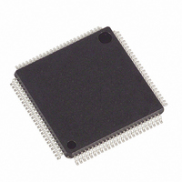
DS21352L+ Maxim Integrated Products, DS21352L+ Datasheet - Page 80

DS21352L+
Manufacturer Part Number
DS21352L+
Description
IC TXRX T1 1-CHIP 3.3V 100-LQFP
Manufacturer
Maxim Integrated Products
Datasheet
1.DS21352L.pdf
(137 pages)
Specifications of DS21352L+
Function
Single-Chip Transceiver
Interface
HDLC, T1
Number Of Circuits
1
Voltage - Supply
3.14 V ~ 3.47 V
Current - Supply
75mA
Operating Temperature
0°C ~ 70°C
Mounting Type
Surface Mount
Package / Case
100-LQFP
Includes
DSX-1 and CSU Line Build-Out Generator, HDLC Controller, In-Band Loop Code Generator and Detector
Lead Free Status / RoHS Status
Lead free / RoHS Compliant
Power (watts)
-
- Current page: 80 of 137
- Download datasheet (2Mb)
TDC2: TRANSMIT HDLC DS0 CONTROL REGISTER 2 (Address=93 Hex)
15.4 LEGACY FDL SUPPORT
15.4.1 OVERVIEW
In order to provide backward compatibility to the older DS2152 device, the DS21352/552 maintains the
circuitry that existed in the previous generation of the T1 Quad Framer. Sections 15.4.2 and 15.4.3 cover
the circuitry and operation of this legacy functionality. In new applications, it is recommended that the
HDLC controller and BOC controller described in Section 15.3 are used. On the receive side, it is
possible to have both the new HDLC/BOC controller and the legacy hardware working at the same time.
On the transmit side the HDLC/BOC controller can be assigned to a DSO while the legacy function
supports the FDL via software. Software for supporting the legacy functions is available from Dallas
Semiconductor.
15.4.2 RECEIVE SECTION
In the receive section, the recovered FDL bits or Fs bits are shifted bit–by–bit into the Receive FDL
register (RFDL). Since the RFDL is 8 bits in length, it will fill up every 2 ms (8 times 250 us). The framer
will signal an external microcontroller that the buffer has filled via the SR2.4 bit. If enabled via IMR2.4,
the INT pin will toggle low indicating that the buffer has filled and needs to be read. The user has 2 ms to
read this data before it is lost. If the byte in the RFDL matches either of the bytes programmed into the
RFDLM1 or RFDLM2 registers, then the SR2.2 bit will be set to a one and the INT pin will toggled low
if enabled via IMR2.2. This feature allows an external microcontroller to ignore the FDL or Fs pattern
until an important event occurs.
(MSB)
SYMBOL
TDB8
TDB8
TDB7
TDB6
TDB5
TDB4
TDB3
TDB2
TDB1
TDB7
POSITION
TDC2.7
TDC2.6
TDC2.5
TDC2.4
TDC2.3
TDC2.2
TDC2.1
TDC2.0
TDB6
NAME AND DESCRIPTION
DS0 Bit 8 Suppress Enable. MSB of the DS0. Set to one to stop this bit from
being used.
DS0 Bit 7 Suppress Enable. Set to one to stop this bit from being used.
DS0 Bit 6 Suppress Enable. Set to one to stop this bit from being used.
DS0 Bit 5 Suppress Enable. Set to one to stop this bit from being used.
DS0 Bit 4 Suppress Enable. Set to one to stop this bit from being used.
DS0 Bit 3 Suppress Enable. Set to one to stop this bit from being used.
DS0 Bit 2 Suppress Enable. Set to one to stop this bit from being used.
DS0 Bit 1 Suppress Enable. LSB of the DS0. Set to one to stop this bit from
being used.
TDB5
TDB4
80 of 137
TDB3
TDB2
(LSB)
TDB1
Related parts for DS21352L+
Image
Part Number
Description
Manufacturer
Datasheet
Request
R

Part Number:
Description:
MAX7528KCWPMaxim Integrated Products [CMOS Dual 8-Bit Buffered Multiplying DACs]
Manufacturer:
Maxim Integrated Products
Datasheet:

Part Number:
Description:
Single +5V, fully integrated, 1.25Gbps laser diode driver.
Manufacturer:
Maxim Integrated Products
Datasheet:

Part Number:
Description:
Single +5V, fully integrated, 155Mbps laser diode driver.
Manufacturer:
Maxim Integrated Products
Datasheet:

Part Number:
Description:
VRD11/VRD10, K8 Rev F 2/3/4-Phase PWM Controllers with Integrated Dual MOSFET Drivers
Manufacturer:
Maxim Integrated Products
Datasheet:

Part Number:
Description:
Highly Integrated Level 2 SMBus Battery Chargers
Manufacturer:
Maxim Integrated Products
Datasheet:

Part Number:
Description:
Current Monitor and Accumulator with Integrated Sense Resistor; ; Temperature Range: -40°C to +85°C
Manufacturer:
Maxim Integrated Products

Part Number:
Description:
TSSOP 14/A�/RS-485 Transceivers with Integrated 100O/120O Termination Resis
Manufacturer:
Maxim Integrated Products

Part Number:
Description:
TSSOP 14/A�/RS-485 Transceivers with Integrated 100O/120O Termination Resis
Manufacturer:
Maxim Integrated Products

Part Number:
Description:
QFN 16/A�/AC-DC and DC-DC Peak-Current-Mode Converters with Integrated Step
Manufacturer:
Maxim Integrated Products

Part Number:
Description:
TDFN/A/65V, 1A, 600KHZ, SYNCHRONOUS STEP-DOWN REGULATOR WITH INTEGRATED SWI
Manufacturer:
Maxim Integrated Products

Part Number:
Description:
Integrated Temperature Controller f
Manufacturer:
Maxim Integrated Products

Part Number:
Description:
SOT23-6/I�/45MHz to 650MHz, Integrated IF VCOs with Differential Output
Manufacturer:
Maxim Integrated Products

Part Number:
Description:
SOT23-6/I�/45MHz to 650MHz, Integrated IF VCOs with Differential Output
Manufacturer:
Maxim Integrated Products

Part Number:
Description:
EVALUATION KIT/2.4GHZ TO 2.5GHZ 802.11G/B RF TRANSCEIVER WITH INTEGRATED PA
Manufacturer:
Maxim Integrated Products

Part Number:
Description:
QFN/E/DUAL PCIE/SATA HIGH SPEED SWITCH WITH INTEGRATED BIAS RESISTOR
Manufacturer:
Maxim Integrated Products
Datasheet:


