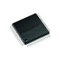
MAX2991ECM+ Maxim Integrated Products, MAX2991ECM+ Datasheet - Page 9

MAX2991ECM+
Manufacturer Part Number
MAX2991ECM+
Description
IC TXRX FRONT-END 48LQFP
Manufacturer
Maxim Integrated Products
Type
General Purposer
Datasheet
1.MAX2991ECM.pdf
(22 pages)
Specifications of MAX2991ECM+
Function
Analog Front-End Transceiver
Interface
SPI Serial
Number Of Circuits
1
Voltage - Supply
3 V ~ 3.6 V
Current - Supply
36mA, 70mA
Power (watts)
1.54W
Operating Temperature
-40°C ~ 85°C
Mounting Type
Surface Mount
Package / Case
48-LQFP
Includes
Automatic Gain Control (AGC)
Product
Analog Front End
Data Rate
1.2 Msps
Interface Type
Digital
Supply Voltage (max)
3.6 V
Supply Voltage (min)
3 V
Supply Current
36 mA, 70 mA
Maximum Operating Temperature
+ 85 C
Minimum Operating Temperature
- 40 C
Maximum Power Dissipation
1535 mW
Mounting Style
SMD/SMT
Number Of Channels
2
Lead Free Status / RoHS Status
Lead free / RoHS Compliant
PIN
Power-Line Communications (PLC) Integrated
14
15
16
17
18
19
20
21
22
23
24
25
26
27
28
29
30
31
32
33
34
35
36
37
38
39
40
41
42
RXCONV
RBIASRX
RBIASTX
TXCONV
HPFOUT
HPFOUT
RXDATA
REFCLK
TXDATA
AGCCS
SDOUT
TXCLK
RXCLK
NAME
GND3
GND4
GSUB
GND5
SHDN
GND6
SCLK
ENRX
ENTX
SDIN
V
V
V
V
REF
CS
DD3
DD4
DD5
DD6
_______________________________________________________________________________________
Active-High AGC Carrier-Select Enable. Drive AGCCS high to initiate the internal AGC adaptation
timer.
Host SPI Serial-Clock Input
Host SPI Serial-Data Input
Active-Low Host SPI Chip-Select Input
Host SPI Serial-Data Output
Analog Power-Supply 3. Bypass to GND3 with 100nF and 10FF capacitors in parallel located close to
V
Analog Ground 3. Connect GND3 to the PCB ground.
Transmitter Bias. Connect a 25kI resistor with 1% accuracy rating between RBIASTX and the PCB
ground to set the bias current for the transmitter path.
Analog Reference Clock Input
Digital Ground. Connect GND4 to the PCB ground.
Digital Power Supply. Bypass to GND4 with 100nF and 10FF capacitors in parallel located close to
V
Transmit DAC Conversion Start. The beginning of the Tx conversion data frame is signaled by the
falling edge of TXCONV.
Receive ADC Conversion Start. Rx data is sampled by the ADC and conversion begins on the falling
edge of RXCONV.
Transmit Path Serial-Data Input. Data is latched on the falling edge of the TXCLK.
Receive Path Serial-Data Output. Data is clocked out on the falling edge of RXCLK.
Transmit Path Serial Clock
Receive Path Serial Clock
Substrate Ground. Make low resistance and low inductance connection to the PCB ground.
Active-Low Receive Enable. Drive ENRX low to enable the receiver. Drive ENRX high to disable the
receiver.
Active-Low Transmit Enable. Drive ENTX low to enable the transmitter. Drive ENTX high to disable the
transmitter and place predriver outputs into three-state.
Analog Power-Supply 5. Bypass to GND5 with 100nF and 10FF capacitors in parallel located close to
V
Analog Ground 5. Connect GND5 to the PCB ground.
ADC Reference Voltage Output. Internal 2.0V reference output. Bypass REF with parallel 100nF and
10FF capacitors to the ADC ground.
Active-Low Shutdown Input. Drive SHDN low to place the MAX2991 into shutdown mode. Drive
SHDN high for normal operation.
Receive Bias. RBIASRX is the external resistor connection that sets the bias current for the receive
path. Connect a 25kI resistor with 1% accuracy rating between RBIASRX and the PCB ground.
Analog Ground 6. Connect GND6 to the PCB ground.
Analog Power-Supply 6. Bypass to GND6 with parallel 100nF and 10FF capacitors located close to
V
Highpass Filter Negative Output
Highpass Filter Positive Output
DD3
DD4
DD5
DD6
. Connect V
. Connect V
. Connect V
. Connect V
DD
DD
DD
DD
inputs together.
inputs together.
inputs together.
inputs together.
Analog Front-End Transceiver
FUNCTION
Pin Description (continued)
9


