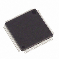
DS21Q50L Maxim Integrated Products, DS21Q50L Datasheet - Page 74

DS21Q50L
Manufacturer Part Number
DS21Q50L
Description
IC TRANSCEIVER E1 QUAD 100-LQFP
Manufacturer
Maxim Integrated Products
Datasheet
1.DS21Q50L.pdf
(87 pages)
Specifications of DS21Q50L
Function
Transceiver
Interface
E1
Number Of Circuits
4
Voltage - Supply
3.14 V ~ 3.47 V
Current - Supply
230mA
Operating Temperature
0°C ~ 70°C
Mounting Type
Surface Mount
Package / Case
100-LQFP
Includes
AIS Alarms Detector and Generator, Loopback Functions, PRBS Generator / Detector, Remote Detector and Generator
Lead Free Status / RoHS Status
Contains lead / RoHS non-compliant
Power (watts)
-
Available stocks
Company
Part Number
Manufacturer
Quantity
Price
Part Number:
DS21Q50L
Manufacturer:
MAXIM/美信
Quantity:
20 000
Company:
Part Number:
DS21Q50L+
Manufacturer:
SPANSION
Quantity:
119
Company:
Part Number:
DS21Q50L+
Manufacturer:
MAXIM
Quantity:
3
Company:
Part Number:
DS21Q50L-W+
Manufacturer:
Maxim Integrated
Quantity:
10 000
Note 1:
Note 2:
Note 3:
Note 4:
20.
ABSOLUTE MAXIMUM RATINGS
Voltage Range on Any Pin Relative to Ground………………………………………………………………-1.0V to +6.0V
Operating Temperature Range for DS21Q50L………………………………………………………………..0°C to +70°C
Operating Temperature Range for DS21Q50LN……………………………………………………………-40°C to +85°C
Storage Temperature Range………………………………………………………………………………...-55°C to +125°C
Soldering Temperature………………………………………………………..See IPC/JEDEC J-STD-020A Specification
Stresses beyond those listed under “Absolute Maximum Ratings” may cause permanent damage to the device. These are stress ratings only,
and functional operation of the device at these or any other conditions beyond those indicated in the operational sections of the specifications is
not implied. Exposure to the absolute maximum rating conditions for extended periods may affect device reliability.
RECOMMENDED DC OPERATING CONDITIONS
(T
Logic 1
Logic 0
Supply (Note 1)
CAPACITANCE
(T
Input Capacitance
Output Capacitance
DC CHARACTERISTICS
(V
Supply Current at 3.3V (Note 2)
Input Leakage (Note 3)
Output Leakage (Note 4)
Output Current (2.4V)
Output Current (0.4V)
A
A
DD
= 0°C to +70°C for DS21Q50L; -40°C to +85°C for DS21Q50LN.)
= +25°C)
= 3.3V ±5%, T
OPERATING PARAMETERS
Applies to RVDD, TVDD, and DVDD.
TCLKs = SYSCLKs = MCLK = 2.048MHz; outputs open circuited; TTIPs and TRINGs driving 30W; QRSS data pattern. 0.0V < V
V
Applies to output pins in tri-state condition.
Applied to INT when tri-stated.
DD
PARAMETER
PARAMETER
.
PARAMETER
A
= 0°C to +70°C for DS21Q50L; V
SYMBOL
SYMBOL
SYMBOL
C
C
I
I
V
I
I
I
V
V
OUT
DD
OH
LO
OL
IL
IN
DD
IH
IL
74 of 87
DD
= 3.3V ±5%, T
3.135
MIN
MIN
MIN
+4.0
-0.3
-1.0
-1.0
2.0
A
= -40°C to +85°C for DS21Q50LN.)
TYP
TYP
TYP
230
3.3
5
7
MAX
MAX
MAX
3.465
+0.8
+1.0
+1.0
5.5
UNITS
UNITS
UNITS
mA
mA
mA
mA
mA
pF
pF
V
V
V
IN
<


