PC16552DV/NOPB National Semiconductor, PC16552DV/NOPB Datasheet - Page 16
PC16552DV/NOPB
Manufacturer Part Number
PC16552DV/NOPB
Description
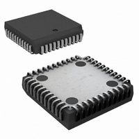
IC UART DUAL WITH FIFO 44-PLCC
Manufacturer
National Semiconductor
Datasheet
1.PC16552DVNOPB.pdf
(22 pages)
Specifications of PC16552DV/NOPB
Features
False-start Bit Detection
Number Of Channels
2, DUART
Fifo's
16 Byte
Voltage - Supply
5V
With False Start Bit Detection
Yes
With Modem Control
Yes
Mounting Type
Surface Mount
Package / Case
44-LCC (J-Lead)
No. Of Channels
2
Data Rate
1.5Mbps
Uart Features
Independently Controlled Transmit, Receive, Line Status, And Data Set Interrupts
Supply Voltage Range
4.5V To 5.5V
Rohs Compliant
Yes
Lead Free Status / RoHS Status
Lead free / RoHS Compliant
Other names
*PC16552DV
*PC16552DV/NOPB
PC16552DV
*PC16552DV/NOPB
PC16552DV
Available stocks
Company
Part Number
Manufacturer
Quantity
Price
Company:

Part Number:
PC16552DV/NOPB
Manufacturer:
TI
Quantity:
7 782
Company:
Part Number:
PC16552DV/NOPB
Manufacturer:
NSC
Quantity:
12 464
Company:
Part Number:
PC16552DV/NOPB
Manufacturer:
Texas Instruments
Quantity:
10 000


8 0 Registers
Note 1 Boldface bits are permanently low
Note 2 Bits 7–4 are driven by the input signals
8 3 PROGRAMMABLE BAUD GENERATOR
The DUART contains two independently programmable
Baud Generators Each is capable of taking a common
clock input from DC to 24 0 MHz and dividing it by any divi-
sor from 1 to 2
recommended with a divisor
frequency of the Baud Generator is 16
output of each Baud Generator drives the transmitter and
receiver sections of the associated serial channel Two 8-bit
latches per channel store the divisor in a 16-bit binary for-
mat These Divisor Latches must be loaded during initializa-
tion to ensure proper operation of the Baud Generator
Upon loading either of the Divisor Latches a 16-bit Baud
Counter is loaded
Table IV provides decimal divisors to use with crystal fre-
quencies of 1 8432 MHz 3 072 MHz and 18 432 MHz For
baud rates of 38400 and below the error obtained is mini-
mal The accuracy of the desired baud rate is dependent on
the crystal frequency chosen Using a divisor of zero is not
recommended
8 4 LINE STATUS REGISTER
This register provides status information to the CPU con-
cerning the data transfer Table II shows the contents of the
Line Status Register Details on each bit follow
Bit 0 This bit is the receiver Data Ready (DR) indicator Bit
0 is set to a logic 1 whenever a complete incoming charac-
ter has been received and transferred into the Receiver
Buffer Register or the FIFO Bit 0 is reset to a logic 0 by
reading all of the data in the Receiver Buffer Register or the
FIFO
Bit 1 This bit is the Overrun Error (OE) indicator Bit 1 indi-
cates that the next character received was transferred into
the Receiver Buffer Register before the CPU could read the
previously received character This transfer destroys the
divisor
Interrupt Enable Register
Interrupt Identification Register
FIFO Control
Line Control Register
MODEM Control Register
Line Status Register
MODEM Status Register
Alternate Function Register
SOUT
INTR (RCVR Errs)
INTR (RCVR Data Ready)
INTR (THRE)
INTR (Modem Status Changes)
OUT 2
RTS
DTR
RCVR FIFO
XMIT FIFO
e
Register Signal
(frequency input)
16
b
1 The highest input clock frequency
(Continued)
e
d
1 is 24 MHz The output
(baud rate
c
TABLE III DUART Reset Configuration
the baud rate
c
16) The
MR FCR1 FCR0
MR FCR1 FCR0
Read IIR Write THR MR
Read MSR MR
Read RBR MR
Reset Control
Read LSR MR
Master Reset
Master Reset
Master Reset
Master Reset
Master Reset
Master Reset
Master Reset
Master Reset
Master Reset
Master Reset
Master Reset
Master Reset
16
previous character The OE indicator is set to a logic 1 dur-
ing the character stop bit time when the overrun condition
exists It is reset whenever the CPU reads the contents of
the Line Status Register If the FIFO mode data continues to
fill the FIFO beyond the trigger level an overrun error will
occur only after the FIFO is full and the next character has
been completely received in the shift register OE is indicat-
ed to the CPU as soon as it happens The character in the
shift register can be overwritten but it is not transferred to
the FIFO
Bit 2 This bit is the Parity Error (PE) indicator Bit 2 indi-
cates that the received data character does not have the
correct even or odd parity as selected by the even-parity-
select bit The PE bit is set to a logic 1 during the character
Stop bit time when the character has a parity error It is
reset to a logic 0 whenever the CPU reads the contents of
the Line Status Register or when the next character is load-
ed into the Receiver Buffer Register In the FIFO mode this
error is associated with the particular character in the FIFO
it applies to This error is revealed to the CPU when its
associated character is at the top of the FIFO
Bit 3 This bit is the Framing Error (FE) indicator Bit 3 indi-
cates that the received character did not have a valid Stop
bit The FE bit is set to a logic 1 when the serial channel
detects a logic 0 during the first Stop bit time The FE indica-
tor is reset whenever the CPU reads the contents of the
Line Status Register or when the next character is loaded
into the Receiver Buffer Register In the FIFO Mode this
error is associated with the particular character in the FIFO
it applies to This error is revealed to the CPU when its
associated character is at the top of the FIFO The serial
channel will try to resynchronize after a framing error To do
this it assumes that the framing error was due to the next
start bit so it samples this ‘‘start’’ bit twice and then takes in
the ‘‘data’’
FCR0
FCR0
0000 0000 (Note 1)
0000 0001
0000 0000
0000 0000
0000 0000
0110 0000
XXXX 0000 (Note 2)
0000 0000
High
Low
Low
Low
Low
High
High
High
All Bits Low
All Bits Low
Reset State
Related parts for PC16552DV/NOPB
Image
Part Number
Description
Manufacturer
Datasheet
Request
R

Part Number:
Description:
UART IC
Manufacturer:
National Semiconductor
Datasheet:

Part Number:
Description:
National Semiconductor [8-Bit D/A Converter]
Manufacturer:
National Semiconductor
Datasheet:
Part Number:
Description:
National Semiconductor [Media Coprocessor]
Manufacturer:
National Semiconductor
Datasheet:
Part Number:
Description:
Digitally Controlled Tone and Volume Circuit with Stereo Audio Power Amplifier, Microphone Preamp Stage and National 3D Sound
Manufacturer:
National Semiconductor
Datasheet:
Part Number:
Description:
Digitally Controlled Tone and Volume Circuit with Stereo Audio Power Amplifier, Microphone Preamp Stage and National 3D Sound
Manufacturer:
National Semiconductor
Datasheet:
Part Number:
Description:
AC97 Rev 2 Codec with Sample Rate Conversion and National 3D Sound
Manufacturer:
National Semiconductor
Part Number:
Description:
Manufacturer:
National Semiconductor
Datasheet:
Part Number:
Description:
Manufacturer:
National Semiconductor
Datasheet:
Part Number:
Description:
General Purpose, Low Voltage, Low Power, Rail-to-Rail Output Operational Amplifiers
Manufacturer:
National Semiconductor
Datasheet:
Part Number:
Description:
8-bit 20 MSPS flash A/D converter.
Manufacturer:
National Semiconductor
Datasheet:
Part Number:
Description:
Low Noise Quad Operational Amplifier
Manufacturer:
National Semiconductor
Datasheet:
Part Number:
Description:
Quad Differential Line Receivers
Manufacturer:
National Semiconductor
Datasheet:
Part Number:
Description:
Quad High Speed Trapezoidal? Bus Transceiver
Manufacturer:
National Semiconductor
Datasheet:
Part Number:
Description:
Dual Line Receiver
Manufacturer:
National Semiconductor
Datasheet: