PC16552DV/NOPB National Semiconductor, PC16552DV/NOPB Datasheet - Page 4
PC16552DV/NOPB
Manufacturer Part Number
PC16552DV/NOPB
Description
IC UART DUAL WITH FIFO 44-PLCC
Manufacturer
National Semiconductor
Datasheet
1.PC16552DVNOPB.pdf
(22 pages)
Specifications of PC16552DV/NOPB
Features
False-start Bit Detection
Number Of Channels
2, DUART
Fifo's
16 Byte
Voltage - Supply
5V
With False Start Bit Detection
Yes
With Modem Control
Yes
Mounting Type
Surface Mount
Package / Case
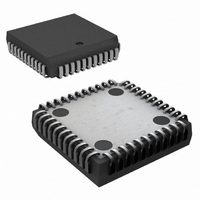
44-LCC (J-Lead)
No. Of Channels
2
Data Rate
1.5Mbps
Uart Features
Independently Controlled Transmit, Receive, Line Status, And Data Set Interrupts
Supply Voltage Range
4.5V To 5.5V
Rohs Compliant
Yes
Lead Free Status / RoHS Status
Lead free / RoHS Compliant
Other names
*PC16552DV
*PC16552DV/NOPB
PC16552DV
*PC16552DV/NOPB
PC16552DV
Available stocks
Company
Part Number
Manufacturer
Quantity
Price
Company:

Part Number:
PC16552DV/NOPB
Manufacturer:
TI
Quantity:
7 782
Company:
Part Number:
PC16552DV/NOPB
Manufacturer:
NSC
Quantity:
12 464
Company:
Part Number:
PC16552DV/NOPB
Manufacturer:
Texas Instruments
Quantity:
10 000


BAUD GENERATOR
RECEIVER
Symbol
t
t
t
t
t
t
t
t
t
t
t
t
t
t
t
RC
WC
N
t
t
t
t
t
t
t
3 0 AC Electrical Characteristics
AR
AW
DH
DS
HZ
MR
RA
RC
RD
RVD
WA
WC
WR
XH
XL
BHD
BLD
RAI
RINT
RXI
SCD
SINT
Note 1 In the FIFO mode (FCR0
indication will be delayed 3 RCLKs Status indicators (PE FE BI) will be delayed 3 RCLKs after the first byte has been received For subsequently received bytes
these indicators will be updated immediately after RDRBR goes inactive Timeout interrupt is delayed 8 RCLKs
Note 2 Charge and discharge time is determined by V
Note 3 All AC timings can be met with current loads that don’t exceed 3 2 mA or
Note 4 For capacitive loads that exceed 100 pF the following typical derating factors should be used
100 pF
150 pF
RD Delay from Address
WR Delay from Address
Data Hold Time
Data Setup Time
RD to Floating Data Delay
Master Reset Pulse Width
Address Hold Time from RD
Read Cycle Update
RD Strobe Width
Delay from RD to Data
Address Hold Time from WR
Write Cycle Update
WR Strobe Width
Duration of Clock High Pulse
Duration of Clock Low Pulse
Read Cycle
Write Cycle
Baud Divisor
Baud Output Positive Edge Delay
Baud Output Negative Edge Delay
Delay from Active Edge of RD to
Reset Interrupt
Delay from Inactive Edge of RD
(RD LSR)
to Reset Interrupt
Delay from READ to RXRDY Inactive
Delay from RCLK to Sample Time
Delay from Stop to Set Interrupt
k
k
I
I
Limits I
SINK
SOURCE
C
C
L s
L s
SOURCE
150 pF t
200 pF t
e
e
Parameter
t
t
t
t
is negative I
AW
e
e
AR
e
e
e
(0 1 ns pF)(C
(0 08 ns pF)(C
(0 5 ns mA)(I
(0 5 ns mA)(I
1) the trigger level interrupts the receiver data available indication the active RXRDY indication and the overrun error
a
a
t
t
RD
WR
SINK s
a
a
L
t
SINK
SOURCE
RC
t
L
WC
b
b
OL
4 8 mA I
100 pF)
mA)
100 pF)
V
OH
mA)
and the external loading
SOURCE s
External Clock (24 MHz Max)
External Clock (24 MHz Max)
T
A
e
f
f
b
X
X
0 C to
120 A C
e
e
Conditions
4
(Note 2)
(Note 1)
24 MHz
24 MHz
b
80 A at 100 pF capacitive loading
a
70 C V
L s
d
d
250 pF
2
2
DD
e a
AC Testing Load Circuit
5V
g
Min
500
15
15
15
10
29
40
29
40
17
17
84
84
10%
5
0
0
1
2
16
Max
20
25
45
45
78
40
55
33
2
b
1
TL C 9426 – 22
BAUDOUT
Cycles
Units
ns
ns
ns
ns
ns
ns
ns
ns
ns
ns
ns
ns
ns
ns
ns
ns
ns
ns
ns
ns
ns
ns
ns
Related parts for PC16552DV/NOPB
Image
Part Number
Description
Manufacturer
Datasheet
Request
R

Part Number:
Description:
UART IC
Manufacturer:
National Semiconductor
Datasheet:

Part Number:
Description:
National Semiconductor [8-Bit D/A Converter]
Manufacturer:
National Semiconductor
Datasheet:
Part Number:
Description:
National Semiconductor [Media Coprocessor]
Manufacturer:
National Semiconductor
Datasheet:
Part Number:
Description:
Digitally Controlled Tone and Volume Circuit with Stereo Audio Power Amplifier, Microphone Preamp Stage and National 3D Sound
Manufacturer:
National Semiconductor
Datasheet:
Part Number:
Description:
Digitally Controlled Tone and Volume Circuit with Stereo Audio Power Amplifier, Microphone Preamp Stage and National 3D Sound
Manufacturer:
National Semiconductor
Datasheet:
Part Number:
Description:
AC97 Rev 2 Codec with Sample Rate Conversion and National 3D Sound
Manufacturer:
National Semiconductor
Part Number:
Description:
Manufacturer:
National Semiconductor
Datasheet:
Part Number:
Description:
Manufacturer:
National Semiconductor
Datasheet:
Part Number:
Description:
General Purpose, Low Voltage, Low Power, Rail-to-Rail Output Operational Amplifiers
Manufacturer:
National Semiconductor
Datasheet:
Part Number:
Description:
8-bit 20 MSPS flash A/D converter.
Manufacturer:
National Semiconductor
Datasheet:
Part Number:
Description:
Low Noise Quad Operational Amplifier
Manufacturer:
National Semiconductor
Datasheet:
Part Number:
Description:
Quad Differential Line Receivers
Manufacturer:
National Semiconductor
Datasheet:
Part Number:
Description:
Quad High Speed Trapezoidal? Bus Transceiver
Manufacturer:
National Semiconductor
Datasheet:
Part Number:
Description:
Dual Line Receiver
Manufacturer:
National Semiconductor
Datasheet: