PC16552DV/NOPB National Semiconductor, PC16552DV/NOPB Datasheet - Page 20
PC16552DV/NOPB
Manufacturer Part Number
PC16552DV/NOPB
Description
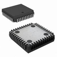
IC UART DUAL WITH FIFO 44-PLCC
Manufacturer
National Semiconductor
Datasheet
1.PC16552DVNOPB.pdf
(22 pages)
Specifications of PC16552DV/NOPB
Features
False-start Bit Detection
Number Of Channels
2, DUART
Fifo's
16 Byte
Voltage - Supply
5V
With False Start Bit Detection
Yes
With Modem Control
Yes
Mounting Type
Surface Mount
Package / Case
44-LCC (J-Lead)
No. Of Channels
2
Data Rate
1.5Mbps
Uart Features
Independently Controlled Transmit, Receive, Line Status, And Data Set Interrupts
Supply Voltage Range
4.5V To 5.5V
Rohs Compliant
Yes
Lead Free Status / RoHS Status
Lead free / RoHS Compliant
Other names
*PC16552DV
*PC16552DV/NOPB
PC16552DV
*PC16552DV/NOPB
PC16552DV
Available stocks
Company
Part Number
Manufacturer
Quantity
Price
Company:

Part Number:
PC16552DV/NOPB
Manufacturer:
TI
Quantity:
7 782
Company:
Part Number:
PC16552DV/NOPB
Manufacturer:
NSC
Quantity:
12 464
Company:
Part Number:
PC16552DV/NOPB
Manufacturer:
Texas Instruments
Quantity:
10 000


8 0 Registers
Bits 1 and 2 These select the output signal that will be
present on the multi-function pin MF These bits are individ-
ually programmable for each channel so that different sig-
nals can be selected on each channel Table VI associates
the signal present at the multi-function pin with the bit code
Note 1 This is the state after power-up or master reset
Note 2 Output is forced high
Bits 3 through 7 These bits are permanently set to a logic
0
8 11 SCRATCHPAD REGISTER
This 8-bit Read Write Register does not control the serial
channel in any way It is intended as a Scratchpad Register
to be used by the programmer to hold data temporarily
9 0 FIFO Mode Operation
Each serial channel has two 16-byte FIFOs associated with
it The operational description that follows is applicable to
the FIFOs of both channels
9 1 FIFO INTERRUPT OPERATION
When the RCVR FIFO and receiver interrupt are enabled
(FCR0
will occur as follows
A The Receive Data Available Interrupt will be issued to the
B The IIR Receive Data Available Indication also occurs
C The Receiver Line Status Interrupt (IIR
D The data ready bit (LSR0) is set as soon as a character is
When RCVR FIFO and receiver interrupts are enabled
RCVR FIFO timeout interrupts will occur as follows
A A RCVR FIFO Timeout Interrupt will occur if the following
Bit 2
CPU when the number of bytes in the RCVR FIFO equals
the programmed trigger level it will be cleared as soon
as the number of bytes in the RCVR FIFO drops below its
programmed trigger level
when the FIFO trigger level is reached and like the inter-
rupt it is cleared when the FIFO drops below the trigger
level
conditions exist
has higher priority than the Received Data Available
(IIR
transferred from the shift register to the RCVR FIFO It is
reset when the RCVR FIFO is empty
0
0
1
1
at least one character is in the RCVR FIFO
the most recent serial character received was longer
than 4 continuous character times ago (if 2 stop bits
are programmed the second one is included in this
time delay)
the most recent CPU read of the RCVR FIFO was
longer than 4 continuous character times ago
AFR Bit Code
e
e
Bit 1
04) Interrupt
0
1
0
1
1 IER0
(Note 1)
e
1) Receive Data Available Interrupts
(Continued)
TABLE VI
OUT 2
BAUDOUT
RXRDY
Reserved
Multi-Function Pin Signal
e
06) as before
(Note 2)
20
B Character times are calculated by using the BAUDOUT
C When a timeout interrupt has occurred it is cleared and
D When the timeout interrupt indication is inactive the time-
When the XMIT FIFO interrupts are enabled (FCR0
IER1
A The Transmitter Holding Register Empty Interrupt occurs
B The transmitter FIFO empty indications will be delayed 1
This delay prevents the DUART from issuing a second
Transmitter Holding Register Empty Interrupt as soon as it
transfers the first character into the Transmitter Shift Regis-
ter
Character timeout and RCVR FIFO trigger level interrupts
have the same priority as the current received data avail-
able interrupt XMIT FIFO Empty has the same priority as
the current Transmitter Holding Register Empty Interrupt
9 2 FIFO POLLED OPERATION
With FCR0
zero puts the associated serial channel in the FIFO Polled
Mode of operation Since the receiver and transmitter are
controlled separately either one or both can be in the polled
mode of operation
In this mode the user’s program will check receiver and
transmitter status via the LSR As stated in Section 8 4
There is no trigger level reached or timeout condition indi-
cated in the FIFO Polled Mode however the RCVR and
XMIT FIFOs are otherwise functional
The maximum time between a received character and a
timeout interrupt will be 160 ms at 300 baud with a 12-bit
receive character (i e 1 START 8 DATA 1 PARITY and
2 STOP BITS)
signal as a clock signal (this makes the delay proportion-
al to the baud rate)
the timer reset when the CPU reads one character from
the RCVR FIFO
out indication timer is reset after a new character is re-
ceived or after the CPU reads the RCVR FIFO
when the XMIT FIFO is empty It is cleared as soon as
the Transmitter Holding Register is written to (1 to 16
characters may be written to the XMIT FIFO while servic-
ing this interrupt) or the IIR is read
character time minus the last Stop bit time whenever the
following occurs THRE
least two bytes at the same time in the transmit FIFO
since the last THRE
Register Empty Interrupt after changing FCR0 will be im-
mediate if it is enabled
LSR0 will be set as long as there is one byte in the RCVR
FIFO
LSR1 to LSR4 will specify which error(s) has occurred
Character error status is handled the same way as in the
interrupt mode
LSR5 will indicate when the XMIT FIFO is empty
LSR6 will indicate that both the XMIT FIFO and shift reg-
ister are empty
LSR7 will indicate whether there are any errors in the
RCVR FIFO
e
1) XMIT interrupts will occur as follows
e
1 resetting IER0 IER1 IER2 IER3 or all to
e
e
1 The first Transmitter Holding
1 and there have not been at
e
1
Related parts for PC16552DV/NOPB
Image
Part Number
Description
Manufacturer
Datasheet
Request
R

Part Number:
Description:
UART IC
Manufacturer:
National Semiconductor
Datasheet:

Part Number:
Description:
National Semiconductor [8-Bit D/A Converter]
Manufacturer:
National Semiconductor
Datasheet:
Part Number:
Description:
National Semiconductor [Media Coprocessor]
Manufacturer:
National Semiconductor
Datasheet:
Part Number:
Description:
Digitally Controlled Tone and Volume Circuit with Stereo Audio Power Amplifier, Microphone Preamp Stage and National 3D Sound
Manufacturer:
National Semiconductor
Datasheet:
Part Number:
Description:
Digitally Controlled Tone and Volume Circuit with Stereo Audio Power Amplifier, Microphone Preamp Stage and National 3D Sound
Manufacturer:
National Semiconductor
Datasheet:
Part Number:
Description:
AC97 Rev 2 Codec with Sample Rate Conversion and National 3D Sound
Manufacturer:
National Semiconductor
Part Number:
Description:
Manufacturer:
National Semiconductor
Datasheet:
Part Number:
Description:
Manufacturer:
National Semiconductor
Datasheet:
Part Number:
Description:
General Purpose, Low Voltage, Low Power, Rail-to-Rail Output Operational Amplifiers
Manufacturer:
National Semiconductor
Datasheet:
Part Number:
Description:
8-bit 20 MSPS flash A/D converter.
Manufacturer:
National Semiconductor
Datasheet:
Part Number:
Description:
Low Noise Quad Operational Amplifier
Manufacturer:
National Semiconductor
Datasheet:
Part Number:
Description:
Quad Differential Line Receivers
Manufacturer:
National Semiconductor
Datasheet:
Part Number:
Description:
Quad High Speed Trapezoidal? Bus Transceiver
Manufacturer:
National Semiconductor
Datasheet:
Part Number:
Description:
Dual Line Receiver
Manufacturer:
National Semiconductor
Datasheet: