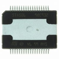
STA50613TR STMicroelectronics, STA50613TR Datasheet
STA50613TR
Specifications of STA50613TR
STA50613TR
Available stocks


Related parts for STA50613TR


STA50613TR Summary of contents
Page 1
... OUT2B 2 IN2B 32 OUT2B M14 1 5 GND2B PowerSO36 Part Number STA506 STA50613TR 32V output power on 8Ω load and cc 36V on 8Ω load in single CC = 32V on 4Ω load. The input pins have threshold pin voltage. L C30 1µF L18 22µH C20 100nF C52 ...
Page 2
STA506 Table 2. Pin Function Pin n. Pin Name 1 GND-SUB Substrate Ground OUT2B Output Half Bridge Positive Supply CC 5 GND2B Negative Supply 6 GND2A Negative Supply Positive Supply ...
Page 3
Table 3. Functional Pin Status Pin name Pin n. FAULT 27 (*) 27 FAULT TRI-STATE 26 TRI-STATE 26 PWRDN 25 PWRDN 25 THWAR 28 (*) 28 THWAR CONFIG 24 (**) 24 CONFIG (*) : The pin is open collector. To ...
Page 4
STA506 Table 4. Absolute Maximum Ratings Symbol V DC Supply Voltage (Pin 4,7,12,15 Maximum Voltage on pins (logic reference) max P Power Dissipation (T tot T Operating Temperature Range Storage and ...
Page 5
Symbol Parameter V Low level input voltage IN-L I High level Input current IN-H I Low level input current IN-L I High level PWRDN pin input PWRDN-H current V Low logical state voltage VLow LOW (pin PWRDN, TRISTATE) (note 1) ...
Page 6
STA506 Figure 4. Test Circuit. Low current dead time = MAX(DTr,DTf) Duty cycle = 50% INxY Figure 5. INxA Figure 6. High Current Dead time for Bridge application = ABS(DTout(A)-DTin(A))+ABS(DTOUT(B)-DTin(B)) Duty cycle=A M58 Q1 DTin(A) OUTA INA M57 Q3 Duty ...
Page 7
TECHNICAL INFO: The STA506 is a dual channel H-Bridge that is able to deliver more than 60W per channel (@ THD=10%) of audio output power in high efficiency. The STA506 converts both DDX and binary-controlled PWM signals into audio ...
Page 8
STA506 – 1) SHUTDOWN mode: with FAULT (pull-up resistor) and TRI-STATE pins independent, an activated fault will disable the device, signaling low at the FAULT output. The device may subsequently be reset to normal operation by toggling the TRI-STATE pin ...
Page 9
Figure 9. STA506 Power Derating Curve Pdiss(W) Figure 10. Typical Single BTL Configurationto Obtain 120W @ THD 10 +3.3V 100nF GND-Clean GND-Reg 100nF 10K X7R CONFIG TH_WAR TH_WAR PWRDN nPWRDN FAULT 10K TRI-STATE ...
Page 10
STA506 Figure 11. Typical Quad Half Bridge Configuration IN1A 29 IN1A +3.3V CONFIG 24 PWRDN PWRDN 25 PROTECTIONS R57 R59 FAULT 27 10K 10K 26 TRI-STATE C58 100nF TH_WAR 28 TH_WAR IN1B 30 IN1B ...
Page 11
Figure 12. THD+N vs Frequency 1 1 0.5 0.5 Vcc=32V Vcc=32V Rl=8ohm Rl=8ohm 0.2 0.2 0.1 0 0.05 0.05 0.02 0.02 0.01 0. 100 100 200 200 500 500 Hz Hz Figure 13. Output ...
Page 12
STA506 Figure 17. PowerSO36 (Slug Up) Mechanical Data & Package Dimensions MIN. TYP. MAX. A 3.25 3.43 A2 3.1 3 0.2 a1 0.030 -0.040 0.0011 b 0.22 0.38 c 0.23 0.32 D 15.8 ...
Page 13
Table 10. Revision History Date Revision December 2003 April 2004 April 2004 June 2004 November 2004 February 2006 1 First Issue 2 Inserted Technical Info and Graphics 3 Small changes in pag 4 and 5 4 Note 2: See relevant ...
Page 14
... STA506 Information in this document is provided solely in connection with ST products. STMicroelectronics NV and its subsidiaries (“ST”) reserve the right to make changes, corrections, modifications or improvements, to this document, and the products and services described herein at any time, without notice. All ST products are sold pursuant to ST’s terms and conditions of sale. ...