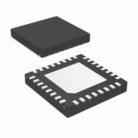
LM49450SQ/NOPB National Semiconductor, LM49450SQ/NOPB Datasheet - Page 22

LM49450SQ/NOPB
Manufacturer Part Number
LM49450SQ/NOPB
Description
IC AUDIO SUBSYSTEM 2.5W D 32LLP
Manufacturer
National Semiconductor
Series
Boomer®r
Type
Class Dr
Datasheet
1.LM49450SQNOPB.pdf
(38 pages)
Specifications of LM49450SQ/NOPB
Output Type
2-Channel (Stereo) with Stereo Headphones
Max Output Power X Channels @ Load
2.5W x 2 @ 4 Ohm
Voltage - Supply
2.7 V ~ 5.5 V
Features
3D, DAC, Depop, I²C, I²S, Mute, Short-Circuit and Thermal Protection, Shutdown, Volume Control
Mounting Type
Surface Mount
Package / Case
32-LLP
Amplifier Class
D
No. Of Channels
2
Output Power
1.2W
Supply Voltage Range
2.7V To 5.5V
Load Impedance
8ohm
Operating Temperature Range
-40°C To +85°C
Amplifier Case Style
LLP
Rohs Compliant
Yes
For Use With
LM49450SQEVAL - BOARD EVAL FOR LM49450
Lead Free Status / RoHS Status
Lead free / RoHS Compliant
Other names
LM49450SQ
LM49450SQ
LM49450SQTR
LM49450SQ
LM49450SQTR
Available stocks
Company
Part Number
Manufacturer
Quantity
Price
Part Number:
LM49450SQ/NOPB
Manufacturer:
TI/德州仪器
Quantity:
20 000
www.national.com
other ACK bit. Following the acknowledgement of the register
data word, the master issues a STOP bit, allowing SDA to go
high while SDA is high.
I
The LM49450 supports three I
ure 5), Left Justified Mode (Figure 6), and Right Justified
GENERAL AMPLIFIER FUNCTION
Class D Amplifier
The LM49450 features a high-efficiency stereo Class D audio
power amplifier that utilizes National’s filterless modulation
scheme which reduces external component count, conserves
board space and reduces system cost. The Class D outputs
transition between V
frequency. With no signal applied, the outputs switch with a
50% duty cycle, in phase, causing the two outputs to cancel.
2
S DATA FORMAT
DD
and GND with a 300kHz switching
2
S formats: Normal Mode (Fig-
FIGURE 7. I
FIGURE 6. I
FIGURE 5. I
2
2
S Right Justified Input Format
S Left Justified Input Format
2
S Normal Input Format
22
Mode (Figure 7). In Normal Mode, the audio data is transmit-
ted MSB first, with the unused bits following the LSB. In Left
Justified Mode, the audio data format is similar to the Normal
Mode, without the delay between the LSB and the change in
I
mitted after a delay of a preset number of bits.
This cancellation results in no net voltage across the speaker,
thus there is no current to the load in the idle state.
With the input signal applied, the duty cycle (pulse width) of
the LM49450 outputs changes. For increasing output voltage,
the duty cycle of V_LS+ increases while the duty cycle of
V_LS- decreases. For decreasing output voltages, the con-
verse occurs. The difference between the two pulse widths
yield the differential output voltage.
2
S_WS. In Right Justified Mode, the audio data MSB is trans-
300455b3
300455b2
300455a9


