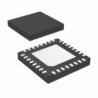
LM49450SQ/NOPB National Semiconductor, LM49450SQ/NOPB Datasheet - Page 34

LM49450SQ/NOPB
Manufacturer Part Number
LM49450SQ/NOPB
Description
IC AUDIO SUBSYSTEM 2.5W D 32LLP
Manufacturer
National Semiconductor
Series
Boomer®r
Type
Class Dr
Datasheet
1.LM49450SQNOPB.pdf
(38 pages)
Specifications of LM49450SQ/NOPB
Output Type
2-Channel (Stereo) with Stereo Headphones
Max Output Power X Channels @ Load
2.5W x 2 @ 4 Ohm
Voltage - Supply
2.7 V ~ 5.5 V
Features
3D, DAC, Depop, I²C, I²S, Mute, Short-Circuit and Thermal Protection, Shutdown, Volume Control
Mounting Type
Surface Mount
Package / Case
32-LLP
Amplifier Class
D
No. Of Channels
2
Output Power
1.2W
Supply Voltage Range
2.7V To 5.5V
Load Impedance
8ohm
Operating Temperature Range
-40°C To +85°C
Amplifier Case Style
LLP
Rohs Compliant
Yes
For Use With
LM49450SQEVAL - BOARD EVAL FOR LM49450
Lead Free Status / RoHS Status
Lead free / RoHS Compliant
Other names
LM49450SQ
LM49450SQ
LM49450SQTR
LM49450SQ
LM49450SQTR
Available stocks
Company
Part Number
Manufacturer
Quantity
Price
Part Number:
LM49450SQ/NOPB
Manufacturer:
TI/德州仪器
Quantity:
20 000
www.national.com
DAC COMPENSATION FILTER REGISTERS (0x09h to
0x0Eh)
DAC Compensation Filter
The LM49450 DAC features a 5 band FIR filter that can be
used as an equalizer for the digital audio path. Registers
0x09h, 0x0Ah, 0x0Bh, 0x0Ch, 0x0Dh, and 0x0Eh provide an
8-bit control for each individual FIR filter.
EXTERNAL COMPONENT SELECTION
The LM49450 uses different supplies for each portion of the
device, allowing for the optimum combination of headroom,
power dissipation and noise immunity. The speaker amplifier
gain stage is powered from V
powered from LSV
plifiers and volume control stages are powered from HPV
The separate power supplies allow the speakers to operate
from a higher voltage for maximum headroom, while the
headphones operate from a lower voltage, improving power
dissipation. HPV
ther improve performance in noisy environments. The I
portion if powered from I
LM49450 to interface with lower voltage digital controllers.
PROPER SELECTION OF EXTERNAL COMPONENTS
Power Supply Bypassing and Filtering
Proper power supply bypassing is critical for low noise per-
formance and high PSRR. Place the supply bypass capaci-
tors as close to the device as possible. Typical applications
employ a voltage regulator with 10µF and 0.1µF bypass ca-
pacitors that increase supply stability. These capacitors do
not eliminate the need for bypassing of the LM49450 supply
pins. A 1µF ceramic capacitor placed close to each supply pin
is recommended.
Bypass Capacitor Selection
The LM49450 internally generates a V
bias voltage. The BYPASS capacitor CBYPASS, improves
PSRR and THD+N by reducing noise at the BYPASS node.
Use a 2.2µF ceramic placed as close to the device as possi-
ble.
REF Capacitor Selection
The LM49450 generates an internal low noise reference volt-
age used by the DAC. For best THD+N performance, bypass
REF with 10µF and 0.1µF ceramic capacitors.
Charge Pump Capacitor Selection
Use low ESR ceramic capacitors (less than 100mΩ) for opti-
mum performance.
DD
DD
may be driven by a linear regulator to fur-
. The headphone amplifiers, input am-
2
CV
DD
, allowing the I
DD
, while the output stage is
DD
/2 common-mode
2
C portion of the
DD
2
C
.
34
Charge Pump Flying Capacitor (C1)
The flying capacitor (C1) affects the load regulation and out-
put impedance of the charge pump. A C1 value that is too low
results in a loss of current drive, leading to a loss of amplifier
headroom. A higher valued C1 improves load regulation and
lowers charge pump output impedance to an extent. Above
2.2µF, the R
of C1 and C2 dominate the output impedance. A lower value
capacitor can be used in systems where low maximum output
power requirements.
Charge Pump Hold Capacitor (C2)
The value and ESR of the hold capacitor (C2) directly affects
the ripple on CPV
put ripple. Decreasing the ESR of C2 reduces both output
ripple and charge pump output impedance. A lower value ca-
pacitor can be used in systems where low maximum output
power requirements.
Input Capacitor Selection
The LM49450 analog inputs require input coupling capaci-
tors. Input capacitors block the DC component of the audio
signal, eliminating any conflict between the DC component of
the audio source and the bias voltage of the LM49450. The
input capacitors create a high-pass filter with the input resis-
tors R
Equation (1) below.
Where the value of R
The input capacitors can also be used to remove low fre-
quency content from the audio signal. Small speakers cannot
reproduce, and may even be damaged by low frequencies.
High pass filtering the audio signal helps protect the speakers.
When the LM49450 is using a single-ended source, power
supply noise on the ground is seen as an input signal. Setting
the high-pass filter point above the power supply noise fre-
quencies, 217Hz in a GSM phone, for example, filters out the
noise such that it is not amplified and heard on the output.
Capacitors with a tolerance of 10% or better are recommend-
ed for impedance matching and improved CMRR and PSRR.
IN
. The -3dB point of the high pass filter is found using
DS(ON)
SS
of the charge pump switches and the ESR
f = 1 / 2
. Increasing the value of C2 reduces out-
IN
is typically 20kΩ.
π
R
IN
C
IN
(1)


