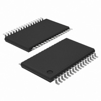
TDA8933BTW/N2,512 NXP Semiconductors, TDA8933BTW/N2,512 Datasheet - Page 5

TDA8933BTW/N2,512
Manufacturer Part Number
TDA8933BTW/N2,512
Description
IC AMP AUDIO 20.6W STER 32TSSOP
Manufacturer
NXP Semiconductors
Type
Class Dr
Datasheet
1.TDA8933BTWN2118.pdf
(42 pages)
Specifications of TDA8933BTW/N2,512
Output Type
1-Channel (Mono) or 2-Channel (Stereo)
Max Output Power X Channels @ Load
20.6W x 1 @ 16 Ohm; 10.3W x 2 @ 8 Ohm
Voltage - Supply
10 V ~ 36 V, ±5 V ~ 18 V
Features
Depop, Differential Inputs, Mute, Short-Circuit and Thermal Protection
Mounting Type
Surface Mount
Package / Case
32-TSSOP Exposed Pad, 32-eTSSOP, 32-HTSSOP
Lead Free Status / RoHS Status
Lead free / RoHS Compliant
Other names
935285222512
TDA8933BTW/N2
TDA8933BTW/N2
TDA8933BTW/N2
TDA8933BTW/N2
NXP Semiconductors
8. Functional description
TDA8933B_1
Preliminary data sheet
8.1 General
Table 3.
[1]
The TDA8933B is a mono full-bridge or stereo half-bridge audio power amplifier using
class D technology. The audio input signal is converted into a PWM signal via an analog
input stage and a PWM modulator. To enable the output power Diffusion Metal Oxide
Semiconductor (DMOS) transistors to be driven, this digital PWM signal is applied to a
control and handshake block and driver circuits for both the high side and low side. A
2
signal across the loudspeakers.
The TDA8933B contains two independent half bridges with full differential input stages.
The loudspeakers can be connected in the following configurations:
The TDA8933B contains circuits common to both channels such as the oscillator, all
reference sources, the mode functionality and a digital timing manager. The following
protections are built-in: thermal foldback and overtemperature, current and voltage
protections.
Symbol
HVP2
V
BOOT2
OUT2
V
STAB2
STAB1
V
OUT1
BOOT1
V
HVP1
OSCIO
V
Exposed die
pad
nd
•
•
DDP2
SSP2
SSP1
DDP1
SSD(HW)
-order low-pass filter in the application converts the PWM signal to an analog audio
[1]
The exposed die pad has to be connected to V
Mono full-bridge: Bridge-Tied Load (BTL)
Stereo half-bridge: Single-Ended (SE)
Pinning description
Pin
19
20
21
22
23
24
25
26
27
28
29
30
31
32
-
Rev. 01 — 23 October 2008
Description
half supply output voltage 2 for charging single-ended capacitor for
channel 2
positive power supply voltage for channel 2
bootstrap high-side driver channel 2
Pulse Width Modulated (PWM) output channel 2
negative power supply voltage for channel 2
decoupling of internal 11 V regulator for channel 2 drivers
decoupling of internal 11 V regulator for channel 1 drivers
negative power supply voltage for channel 1
PWM output channel 1
bootstrap high-side driver for channel 1
positive power supply voltage for channel 1
half supply output voltage 1 for charging single-ended capacitor for
channel 1
oscillator input in slave configuration or oscillator output in master
configuration
negative digital supply voltage and handle wafer connection
…continued
SSD(HW)
.
Class D audio amplifier
TDA8933B
© NXP B.V. 2008. All rights reserved.
5 of 42


