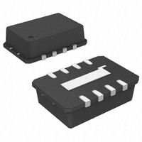
AD8317ACPZ-R7 Analog Devices Inc, AD8317ACPZ-R7 Datasheet - Page 14

AD8317ACPZ-R7
Manufacturer Part Number
AD8317ACPZ-R7
Description
IC AMP LOG DETECT 8GHZ 8-LFCSP
Manufacturer
Analog Devices Inc
Type
Logarithmic Amplifierr
Datasheet
1.AD8317ACPZ-R7.pdf
(20 pages)
Specifications of AD8317ACPZ-R7
Applications
Receiver Signal Strength Indication (RSSI)
Mounting Type
Surface Mount
Package / Case
8-LFCSP
No. Of Amplifiers
1
Dynamic Range, Decades
55
Response Time
20ns
Supply Voltage Range
3V To 5.5V
Amplifier Case Style
LFCSP
No. Of Pins
8
Supply Current
22mA
Lead Free Status / RoHS Status
Lead free / RoHS Compliant
Other names
AD8317ACPZ-R7TR
AD8317
Figure 31 shows the transfer function of the output power vs.
the setpoint voltage over temperature for a 900 MHz sine wave
with an input power of −1.5 dBm. Note that the power control
of the AD8317 has a negative sense. Decreasing V
corresponds to demanding a higher signal from the ADL5330,
increases gain.
The AGC loop is capable of controlling signals just under the
full 60 dB gain control range of the ADL5330. The performance
over temperature is most accurate over the highest power range,
where it is generally most critical. Across the top 40 dB range
of output power, the linear conformance error is well within
±0.5 dB over temperature.
Figure 31. ADL5330 Output Power vs. AD8317 Setpoint Voltage, P
–10
–20
–30
–40
–50
30
20
10
0
0.2
0.4
Figure 30. AD8317 Operating in Controller Mode to Provide Automatic Gain Control Functionality in Combination with the ADL5330
0.6
SETPOINT VOLTAGE (V)
0.8
RF INPUT
SIGNAL
1.0
1.2
DAC
1nF
1.4
100pF
100pF
SETPOINT
VOLTAGE
1.6
INHI
INLO
4.12kΩ
1.8
SET
VPSx
+5V
18kΩ
, which
IN
VSET
CLPF
ADL5330
= −1.5 dBm
TADJ
VOUT
GAIN
4
3
2
1
0
–1
–2
–3
–4
AD8317
LOG AMP
10kΩ
COMx
Rev. B | Page 14 of 20
OPLO
OPHI
COMM
VPOS
+5V
INLO
INHI
120nH
+5V
For the AGC loop to remain in equilibrium, the AD8317 must
track the envelope of the ADL5330 output signal and provide
the necessary voltage levels to the ADL5330 gain control input.
Figure 32 shows an oscilloscope screenshot of the AGC loop
depicted in Figure 30. A 100 MHz sine wave with 50% AM
modulation is applied to the ADL5330. The output signal from
the VGA is a constant envelope sine wave with amplitude corre-
sponding to a setpoint voltage at the AD8317 of 1.5 V. Also
shown is the gain control response of the AD8317 to the
changing input envelope.
47nF
47nF
Figure 32. Oscilloscope Screenshot Showing an AM Modulated Input Signal
120nH
100pF
100pF
1
3
52.3Ω
2
CH1 200mV
CH3 50.0mVΩ
ADL5330 OUTPUT
AD8317 OUTPUT
AM MODULATED INPUT
and the Response from the AD8317
DIRECTIONAL
COUPLER
ATTENUATOR
Ch2
200mV
M2.00ms
T
RF OUTPUT
SIGNAL
640.00µs
A CH2
820mV


