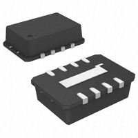
AD8317ACPZ-R7 Analog Devices Inc, AD8317ACPZ-R7 Datasheet - Page 15

AD8317ACPZ-R7
Manufacturer Part Number
AD8317ACPZ-R7
Description
IC AMP LOG DETECT 8GHZ 8-LFCSP
Manufacturer
Analog Devices Inc
Type
Logarithmic Amplifierr
Datasheet
1.AD8317ACPZ-R7.pdf
(20 pages)
Specifications of AD8317ACPZ-R7
Applications
Receiver Signal Strength Indication (RSSI)
Mounting Type
Surface Mount
Package / Case
8-LFCSP
No. Of Amplifiers
1
Dynamic Range, Decades
55
Response Time
20ns
Supply Voltage Range
3V To 5.5V
Amplifier Case Style
LFCSP
No. Of Pins
8
Supply Current
22mA
Lead Free Status / RoHS Status
Lead free / RoHS Compliant
Other names
AD8317ACPZ-R7TR
Figure 33 shows the response of the AGC RF output to a pulse
on VSET. As V
responds with an RF burst. In this configuration, the input
signal to the
of −15 dBm.
Response time and the amount of signal integration are con-
trolled by C
capacitor around an integrating amplifier. Although it is
possible to use large capacitors for C
values under 1 nF provide sufficient filtering.
Calibration in controller mode is similar to the method used
in measurement mode. A simple 2-point calibration can be
done by applying two known V
measuring the output power from the VGA. Slope and intercept
can then be calculated by:
More information on the use of the ADL5330 in AGC applica-
tions can be found in the ADL5330 data sheet.
OUTPUT FILTERING
For applications in which maximum video bandwidth and,
consequently, fast rise time are desired, it is essential that the
CLPF pin be left unconnected and free of any stray capacitance.
The nominal output video bandwidth of 50 MHz can be reduced
by connecting a ground-referenced capacitor (C
pin, as shown in Figure 34. This is generally done to reduce
output ripple (at twice the input frequency for a symmetric
input waveform such as sinusoidal signals).
Slope = (V
Intercept = P
V
1
2
SETx
CH1 2.00V
AD8317 VSET PULSE
ADL5330 OUTPUT
= Slope × (P
T
FLT
ADL5330
Figure 33. Oscilloscope Screenshot Showing
. This functionality is analogous to the feedback
SET
SET1
the Response Time of the AGC Loop
OUT1
decreases from 1.7 V to 0.4 V, the AGC loop
− V
CH2
− V
OUTX
SET2
50mVΩ
is a 1 GHz sine wave at a power level
SET1
)/(P
− Intercept)
/Slope
OUT1
SET
M10.0µs
T
− P
voltages or DAC codes and
FLT
699.800µs
OUT2
, in most applications,
)
A CH1
FLT
) to the CLPF
2.48V
(10)
(11)
Rev. B | Page 15 of 20
(9)
C
The video bandwidth should typically be set to a frequency
equal to about one-tenth the minimum input frequency. This
ensures that the output ripple of the demodulated log output,
which is at twice the input frequency, is well filtered.
In many log amp applications, it may be necessary to lower
the corner frequency of the postdemodulation filter to achieve
low output ripple while maintaining a rapid response time to
changes in signal level. An example of a 4-pole active filter is
shown in the
OPERATION BEYOND 8 GHz
The AD8317 is specified for operation up to 8 GHz, but it provides
useful measurement accuracy over a reduced dynamic range of
up to 10 GHz. Figure 35 shows the performance of the AD8317
over temperature at 10 GHz when the device is configured as
shown in Figure 22. Dynamic range is reduced at this frequency,
but the AD8317 does provide 30 dB of measurement range
within ±3 dB of linearity error.
Implementing an impedance match for frequencies beyond
8 GHz can improve the sensitivity of the AD8317 and measure-
ment range.
Operation beyond 10 GHz is possible, but part-to-part
variation, most notably in the intercept, becomes significant.
FLT
Figure 35. V
is selected by
2.0
1.8
1.6
1.4
1.2
1.0
0.8
0.6
0.4
0.2
C
0
–40
FLT
Figure 34. Lowering the Postdemodulation Bandwidth
=
–35
2 (
OUT
Multiple Devices, R
I
AD8307
LOG
1.5kΩ
π
and Log Conformance vs. Input Amplitude at 10.0 GHz,
×
–30
1
5 .
kΩ
data sheet.
–25
3.5pF
×
Video
–20
P
1
IN
TADJ
AD8317
(dBm)
= Open, C
Bandwidth
–15
+4
–10
LPF
VOUT
CLPF
= 1000 pF
)
–5
−
3
C
5 .
FLT
0
pF
AD8317
5
5
4
3
2
1
0
–1
–2
–3
–4
–5
(12)


