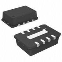
AD8317ACPZ-R7 Analog Devices Inc, AD8317ACPZ-R7 Datasheet - Page 16

AD8317ACPZ-R7
Manufacturer Part Number
AD8317ACPZ-R7
Description
IC AMP LOG DETECT 8GHZ 8-LFCSP
Manufacturer
Analog Devices Inc
Type
Logarithmic Amplifierr
Datasheet
1.AD8317ACPZ-R7.pdf
(20 pages)
Specifications of AD8317ACPZ-R7
Applications
Receiver Signal Strength Indication (RSSI)
Mounting Type
Surface Mount
Package / Case
8-LFCSP
No. Of Amplifiers
1
Dynamic Range, Decades
55
Response Time
20ns
Supply Voltage Range
3V To 5.5V
Amplifier Case Style
LFCSP
No. Of Pins
8
Supply Current
22mA
Lead Free Status / RoHS Status
Lead free / RoHS Compliant
Other names
AD8317ACPZ-R7TR
AD8317
EVALUATION BOARD
Table 5. Evaluation Board (Rev. A) Configuration Options
Component
VPOS, GND
R1, C1, C2
R5, R7
R2, R3, R4, R6, RL, CL
R2, R3
C4, C5
C3
Function
Supply and Ground Connections.
Input Interface.
The 52.3 Ω resistor in Position R1 combines with the internal input impedance
of the AD8317 to give a broadband input impedance of about 50 Ω. C1 and C2
are dc-blocking capacitors. A reactive impedance match can be implemented
by replacing R1 with an inductor and C1 and C2 with appropriately valued
capacitors.
Temperature Compensation Interface.
The internal temperature compensation network is optimized for input signals
up to 3.6 GHz when R7 is 10 kΩ. This circuit can be adjusted to optimize
performance for other input frequencies by changing the value of the resistor
in Position R7. See Table 4 for specific R
Output Interface—Measurement Mode.
In measurement mode, a portion of the output voltage is fed back to the VSET
pin via R2. The magnitude of the slope of the VOUT output voltage response
can be increased by reducing the portion of V
can be used as a back-terminating resistor or as part of a single-pole, low-pass
filter.
Output Interface—Controller Mode.
In this mode, R2 must be open. In controller mode, the AD8317 can control the
gain of an external component. A setpoint voltage is applied to Pin VSET, the
value of which corresponds to the desired RF input signal level applied to the
AD8317 RF input. A sample of the RF output signal from this variable gain
component is selected, typically via a directional coupler, and applied to the
AD8317 RF input. The voltage at the VOUT pin is applied to the gain control of
the variable gain element. A control voltage is applied to the VSET pin. The
magnitude of the control voltage can optionally be attenuated via the voltage
divider comprising R2 and R3, or a capacitor can be installed in Position R3 to
form a low-pass filter along with R2.
Power Supply Decoupling.
The nominal supply decoupling consists of a 100 pF filter capacitor placed
physically close to the AD8317 and a 0.1 μF capacitor placed nearer to the
power supply input pin.
Filter Capacitor.
The low-pass corner frequency of the circuit that drives the VOUT pin can be
lowered by placing a capacitor between CLPF and ground. Increasing this
capacitor increases the overall rise/fall time of the AD8317 for pulsed input
signals. See the Output Filtering section for more details.
RFIN
52.3Ω
R1
47nF
47nF
C1
C2
INLO
INHI
8
1
0.1µF
100pF
Figure 36. Evaluation Board Schematic
C4
C5
VPOS
VPOS
COMM
AD8317
7
2
Rev. B | Page 16 of 20
TADJ
TADJ
CLPF
TADJ
6
3
R5
200Ω
OPEN
C3
8.2pF
R7
resistor values.
VSET
VOUT
OUT
5
4
OPEN
that is fed back to VSET. R6
R3
R4
OPEN
R2
0Ω
VOUT_ALT
1kΩ
R6
GND
CL
OPEN
V
SET
RL
OPEN
V
OUT
Default Conditions
Not applicable
R1 = 52.3 Ω (Size 0402)
C1 = 47 nF (Size 0402)
C2 = 47 nF (Size 0402)
R5 = 200 Ω (Size 0402)
R7 = open (Size 0402)
R2 = 0 Ω (Size 0402)
R3 = open (Size 0402)
R4 = open (Size 0402)
R6 = 1 kΩ (Size 0402)
RL = CL = open (Size 0402)
R2 = open (Size 0402)
R3 = open (Size 0402)
C4 = 0.1 μF (Size 0603)
C5 = 100 pF (Size 0402)
C3 = 8.2 pF (Size 0402)


