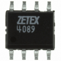
ZXFV4089N8TC Diodes Zetex, ZXFV4089N8TC Datasheet - Page 2

ZXFV4089N8TC
Manufacturer Part Number
ZXFV4089N8TC
Description
IC AMP DC RESTORATION SO8
Manufacturer
Diodes Zetex
Datasheet
1.ZXFV4089N8TC.pdf
(12 pages)
Specifications of ZXFV4089N8TC
Applications
DC Restoration
Number Of Circuits
1
-3db Bandwidth
210MHz
Slew Rate
400 V/µs
Current - Supply
8mA
Current - Output / Channel
40mA
Voltage - Supply, Single/dual (±)
±4.75 V ~ 5.25 V
Mounting Type
Surface Mount
Package / Case
8-SOIC (0.154", 3.90mm Width)
Single Supply Voltage (typ)
Not RequiredV
Dual Supply Voltage (typ)
±5V
Single Supply Voltage (min)
Not RequiredV
Single Supply Voltage (max)
Not RequiredV
Operating Temperature Classification
Industrial
Mounting
Surface Mount
Pin Count
8
Package Type
SOIC
For Use With
ZXFV4583EV - BOARD EVAL FOR ZXFV4583/ZXFV4089
Lead Free Status / RoHS Status
Lead free / RoHS Compliant
Other names
ZXFV4089N8TCTR
Absolute maximum ratings
Positive supply voltage V
Negative supply voltage V
Input voltage, pins 1,2,3 to GND
Differential input voltage 2, pin 1 to pin 2
Output current, pin 7 (continuous, TJ < 110°C)
Internal power dissipation
Input current, IN- pin 1
Current into IN+ and HOLD, pins 2 and 4
Operating ambient temperature range
Storage temperature range
Operating junction temperature T
NOTES:
(b) Stresses above those listed under absolute maximum ratings may cause permanent damage to the device. This is a
(c) At high closed loop gains and low gain setting resistors care must be taken if large input signals are applied to the
(d) The power dissipation of the device when loaded must be designed to keep the device junction temperature below
ESD: This device is sensitive to static discharge and proper handling precautions are required.
Recommended operating conditions
Recommended resistor values
V
Issue 4 - December 2008
© Diodes Incorporated 2008
Parameter
V
V
T
V
R
G
S±
A
S±
CMR
REFCMR
DRIVE
stress rating only; functional operation of the device at these or any other conditions above those indicated in the
operational section of this specification is not implied. Exposure to absolute maximum rating conditions for extended
periods may affect device reliability.
device which cause the output stage to saturate for extended periods of time.
T
1
2
CL
JMAX
= 5V, C
, de-rated according to the Theta-ja for the SO8 package, which is typically 168°C/W, i.e. 0.74W at 25°C.
1000
680
820
430
470
560
R
L
F
Dual supply voltage range
Common mode input voltage range
Ambient temperature range
Common mode input range of V
Effective resistance driving pin 2
= 10pF
430
470
560
n/c
R
G
CC
EE
Peaking
to GND
to GND
1.5dB
2 dB
-2dB
2dB
0
0
JMAX
- Over operating free-air temperature (unless otherwise stated)
REF
2
-0.5V to +5.5V
-5.5V to +0.5V
V
±3 V
±60 mA
See note
±5 mA
±5 mA
-40°C to 85°C
-65°C to 150°C
150°C
EE
-0.5V to V
±4.75
Min.
(d)
-40
30
-3
-2
CC
+0.5V
±5.25
Max.
150
+3
85
+2
ZXFV4089
www.diodes.com
www.zetex.com
Unit
°C
V
V
V
(b)


