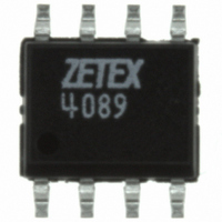
ZXFV4089N8TC Diodes Zetex, ZXFV4089N8TC Datasheet - Page 8

ZXFV4089N8TC
Manufacturer Part Number
ZXFV4089N8TC
Description
IC AMP DC RESTORATION SO8
Manufacturer
Diodes Zetex
Datasheet
1.ZXFV4089N8TC.pdf
(12 pages)
Specifications of ZXFV4089N8TC
Applications
DC Restoration
Number Of Circuits
1
-3db Bandwidth
210MHz
Slew Rate
400 V/µs
Current - Supply
8mA
Current - Output / Channel
40mA
Voltage - Supply, Single/dual (±)
±4.75 V ~ 5.25 V
Mounting Type
Surface Mount
Package / Case
8-SOIC (0.154", 3.90mm Width)
Single Supply Voltage (typ)
Not RequiredV
Dual Supply Voltage (typ)
±5V
Single Supply Voltage (min)
Not RequiredV
Single Supply Voltage (max)
Not RequiredV
Operating Temperature Classification
Industrial
Mounting
Surface Mount
Pin Count
8
Package Type
SOIC
For Use With
ZXFV4583EV - BOARD EVAL FOR ZXFV4583/ZXFV4089
Lead Free Status / RoHS Status
Lead free / RoHS Compliant
Other names
ZXFV4089N8TCTR
Figure 3 shows a portion of a typical video waveform, where the sample pulse is synchronised to
fall within the back porch interval. This can for example be achieved using the Zetex ZXFV4583
sync separator to derive the pulse as in the evaluation circuit described in the data sheet for that
part. Again, during the logic LOW period of the HOLD input, the waveform is driven towards VREF.
Eventually, after a few line scans, the video waveform is stabilised with the back porch level equal
to V
In the video application, the HOLD input state will be HIGH during the picture line sweep and a
negative-going sampling pulse of typically 1.2µs duration will be applied during a central portion
of the back porch interval, so that the back porch or 'Black' level is clamped to V
ground).
If desired, by changing the external pulse timing the signal may be restored such that the sync tip
voltage is clamped to V
In either case, for each line scan, this gives a brightness level consistent with that of the original
camera signal, despite the AC coupling. The value of the coupling capacitor affects two main
characteristics of the circuit:
1. DC level acquisition change
2. DC level droop
DC level acquisition change
In the restore mode the available charging current, together with the capacitor value, determines
the maximum DC voltage correction which can be applied at each sample. For a charging current
limit of 300µA applied for 1.2µs, the charge injected is:
Then the maximum voltage shift correction is:
Issue 4 - December 2008
© Diodes Incorporated 2008
Qmax = 300µA x 1.2µs = 360pC
Vmax = Qmax/C = 360pC / 0.01µF
REF
and this condition is maintained despite any small changes in the input waveform.
= 36mV
REF
instead of the back porch.
Figure 3 Response to typical video signal
8
ZXFV4089
www.diodes.com
www.zetex.com
REF
(typically


