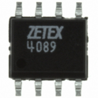
ZXFV4089N8TC Diodes Zetex, ZXFV4089N8TC Datasheet - Page 9

ZXFV4089N8TC
Manufacturer Part Number
ZXFV4089N8TC
Description
IC AMP DC RESTORATION SO8
Manufacturer
Diodes Zetex
Datasheet
1.ZXFV4089N8TC.pdf
(12 pages)
Specifications of ZXFV4089N8TC
Applications
DC Restoration
Number Of Circuits
1
-3db Bandwidth
210MHz
Slew Rate
400 V/µs
Current - Supply
8mA
Current - Output / Channel
40mA
Voltage - Supply, Single/dual (±)
±4.75 V ~ 5.25 V
Mounting Type
Surface Mount
Package / Case
8-SOIC (0.154", 3.90mm Width)
Single Supply Voltage (typ)
Not RequiredV
Dual Supply Voltage (typ)
±5V
Single Supply Voltage (min)
Not RequiredV
Single Supply Voltage (max)
Not RequiredV
Operating Temperature Classification
Industrial
Mounting
Surface Mount
Pin Count
8
Package Type
SOIC
For Use With
ZXFV4583EV - BOARD EVAL FOR ZXFV4583/ZXFV4089
Lead Free Status / RoHS Status
Lead free / RoHS Compliant
Other names
ZXFV4089N8TCTR
ZXFV4089
DC level droop
In the hold state, a small voltage drift is caused by leakage from the sample-hold circuit and bias
current from the main amplifier charging or discharging the coupling capacitor.
The drift rate is equal to the bias/leakage current of up to about 1µA divided by the coupling
capacitor value. For a coupling capacitor of 0.01µF the drift rate is then up to ±100µV/µs.
For a typical video line scan the switch remains open for the rest of the scan duration, or about
62µs. The drift at the end of the line scan has therefore accumulated to about 6.2mV.
This is acceptable for most applications, but if desired it can be reduced by increasing the value
of the coupling capacitor. This will result in a proportionately smaller value of the maximum
available correction voltage at each scan as described above. Normally, once settled, the video
system requires only a very small correction at each scan, so this will not present any problem.
Supply filtering and printed circuit layout
In the applied circuit, the power filtering and printed layout design needs special attention as is
appropriate for a high-speed analog circuit. For each supply lead, use a leadless ceramic chip
capacitor placed very close to the device power pin. A value of 0.1µF is recommended. In addition,
a larger value capacitor, which should be ceramic or solid tantalum construction, with a value of
1 to 10µF, is also recommended for connection to each supply fairly close to the device. The
layout naturally requires some short interconnections on the component side (top copper layer)
and a continuous ground plane should be provided on another layer with plated via holes
providing low inductance ground connections for the device and other components. The
amplifier frequency response is affected to some extent by stray capacitance at the inverting input
at pin 1. This effect can be minimised by providing a small cut-out area in the ground plane and
other layers around pin 1, though this may not always be necessary for the application.
Further Applications Information
The ZXFV4089 is a high speed device requiring the appropriate care in the layout of the
application printed circuit board. A continuous ground plane construction is preferred. Suitable
power supply decoupling suggested includes a 100nF leadless ceramic capacitor close to the
power supply connections at pin 8 and pin 6.
As stated earlier the main video amplifier of the ZXFV4089 is a current feedback amplifier.
Compared to a voltage-feedback amplifier, current feedback provides better bandwidths at higher
gains and also much faster slew rates. To optimize performance from a current feedback amplifier
choice of feedback resistor is very important. In this case, typically the device will be used with a
voltage gain of two, using two resistors of 1k
as in Figure 1. Stray capacitance at the inverting
input node of this circuit can affect frequency and pulse response, so the printed circuit layout
should take account of this. Place the feedback resistors as close as possible to the inverting input
pin and minimize the printed metal connected to this pin.
Common-mode input range
The signal input voltage range is determined partly by the common-mode input range of the main
amplifier. The amplifier configuration is non-inverting, and so the inverting input will follow the
signal input voltage. It is also necessary to observe the maximum limit on the value of V
(±2V)
REF
which is less than the amplifier input voltage range. Therefore the input range of the system is
limited to this value. In addition the restore amplifier voltage input range is restricted to a similar
value.
Issue 4 - December 2008
9
www.zetex.com
www.diodes.com
© Diodes Incorporated 2008


