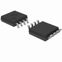
BH76330FVM-TR Rohm Semiconductor, BH76330FVM-TR Datasheet - Page 9

BH76330FVM-TR
Manufacturer Part Number
BH76330FVM-TR
Description
IC VIDEO DVR 6DB CLAMP 8-MSOP
Manufacturer
Rohm Semiconductor
Datasheet
1.BH76362FV-E2.pdf
(33 pages)
Specifications of BH76330FVM-TR
Applications
3:1 Multiplexer-Amplifier
Number Of Circuits
1
Current - Supply
10mA
Voltage - Supply, Single/dual (±)
2.8 V ~ 5.5 V
Mounting Type
Surface Mount
Package / Case
8-TSSOP, 8-MSOP (0.118", 3.00mm Width)
Lead Free Status / RoHS Status
Lead free / RoHS Compliant
Available stocks
Company
Part Number
Manufacturer
Quantity
Price
Company:
Part Number:
BH76330FVM-TR
Manufacturer:
ROHM Semiconductor
Quantity:
135
Part Number:
BH76330FVM-TR
Manufacturer:
ROHM/罗姆
Quantity:
20 000
● Cautions for use
© 2009 ROHM Co., Ltd. All rights reserved.
BH76330FVM, BH76331FVM, BH76360FV, BH76361FV,
BH76332FVM, BH76333FVM, BH76362FV, BH76363FV
www.rohm.com
1. The numerical values and data shown here are typical design values, not guaranteed values.
2. The application circuit examples show recommended circuits, but characteristics should be checked carefully before using
3. Absolute maximum ratings
4. GND potential
5. Thermal design
6. Shorts between pins and mounting errors
7. Operation in strong electromagnetic field
8. Place the power supply's decoupling capacitor as close as possible to the VCC pin (PIN 6) and GND pin (PIN 8).
9. With a clamp input type model (BH76330FVM or BH76332FVM), if any unused input pins are left open they will oscillate, so
10. With models that do not include a 75
11. Frequency response in models that do not include a 75-
3mA
these circuits. If any external part constants are modified before use, factors such as variation in all external parts and
ROHM LSI ICs, including not only static characteristics but also transient characteristics, should be fully considered to set
an ample margin.
If the absolute maximum ratings for applied voltage and/or operation temperature are exceeded, LSI damage may result.
Therefore, do not apply voltage or use in a temperature that exceeds these absolute maximum ratings. If it is possible that
absolute maximum ratings will be exceeded, use a physical safety device such as a fuse and make sure that no conditions
that might exceed the absolute maximum ratings will be applied to the LSI IC.
Regardless of the operation mode, the voltage of the GND pin should be at least the minimum voltage. Actually check
whether or not the voltage at each pin, including transient phenomena, is less than the GND pin voltage.
The thermal design should be done using an ample margin that takes into consideration the allowable dissipation under
actual use conditions.
When mounting LSI ICs onto the circuit board, make sure each LSI's orientation and position is correct. The ICs may
become damaged if they are not mounted correctly when the power is turned on. Similarly, damage may also result if a
short occurs, such as when a foreign object is positioned between pins in an IC, or between a pin and a power supply or
GND connection.
When used within a strong electromagnetic field, evaluate carefully to avoid the risk of operation faults.
unused input pins should instead be connected to GND via a capacitor or else directly connected to VCC.
kH/30 MHz: 0 dB (Typ.) in the application circuit examples (shown in Fig. 9 and Fig. 10), and when resistance of about 1 or
2 k
resistance should be 1 k
and the output resistance of the IC.
set board may cause the peak frequency response to occur at a high frequency. To lower the peak frequency, connect in
series resistors having resistance of several dozen
OUT
(a) Resistor insertion points
is applied from the IC's output pin to GND, this frequency response can be improved (the lower limit of the applied
Fig.16 Positions where Resistors are Inserted to Lower Peak Frequency Response in BH76332FV or BH76333FV
7
Resistance to improve frequency
response (R: 1-2 kΩ)
Fig.17 Result of Resistance Inserted to Improve BH76332FVM/BH76333FVM Frequency Response
). In such cases, gain is reduced, since the output voltage is divided by the added resistance
Other constants are as in application examples (Figs. 9 & 10)
(b) Frequency response changes when resistance is inserted
Input amplitude: 1 Vpp, Output load resistance: 10 kΩ
driver (BH76332FVM or BH76333FVM), in some cases the capacitance added to the
-1
-2
-3
-4
-5
-6
-7
OUT
1
0
1M
7
Output pin
No resistance
Resistors (several dozen Ω to
several hundredΩ) to lower peak
frequency
R=2kΩ
to several hundred
R=1kΩ
10M
Frequency [Hz]
9/32
driver (BH76332FVM and BH76333FVM) was measured as 100
100M
1000M
as close as possible to the output pin.
(c) Voltage gain fluctuation when resistance is inserted
(Voltage gain without inserted resistance: -0.11 dB)
-0.10
-0.12
-0.14
-0.16
-0.18
-0.20
0.5
Resistance added to output pin [k]
出力端子付加抵抗値[kΩ]
1
[f = 100 kHz]
Technical Note
2009.04 - Rev.A
1.5
2
2.5


