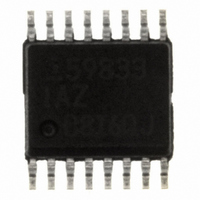
ISL59833IAZ Intersil, ISL59833IAZ Datasheet - Page 11

ISL59833IAZ
Manufacturer Part Number
ISL59833IAZ
Description
IC VIDEO DRIVER TRUE SGL 16-QSOP
Manufacturer
Intersil
Datasheet
1.ISL59833IAZ.pdf
(15 pages)
Specifications of ISL59833IAZ
Applications
Voltage Feedback
Output Type
Rail-to-Rail
Number Of Circuits
3
-3db Bandwidth
200MHz
Slew Rate
500 V/µs
Current - Supply
97mA
Current - Output / Channel
80mA
Voltage - Supply, Single/dual (±)
3 V ~ 3.6 V
Mounting Type
Surface Mount
Package / Case
16-QSOP
Lead Free Status / RoHS Status
Lead free / RoHS Compliant
Available stocks
Company
Part Number
Manufacturer
Quantity
Price
Company:
Part Number:
ISL59833IAZ
Manufacturer:
Intersil
Quantity:
97
Company:
Part Number:
ISL59833IAZ
Manufacturer:
Intersil
Quantity:
75
Part Number:
ISL59833IAZ-T7
Manufacturer:
INTERSIL
Quantity:
20 000
Demo Board Schematic
Description of Operation and Application
Information
Theory Of Operation
The ISL59833 is a highly practical and robust marriage of
three high bandwidth, high speed, low power, rail-to-rail
voltage feedback amplifiers with a charge pump to provide a
negative rail without an additional power supply. Designed to
operate with a single supply voltage range from 0V to 3.3V,
the ISL59833 eliminates the need for a split supply with the
incorporation of a charge pump capable of generating a
bottom rail as much as 1.6V below ground for a 4.9V range
on a single 3.3V supply. This performance is ideal for NTSC
video with its negative-going sync pulses.
THE AMPLIFIER
The ISL59833 fabricated on a di-electrically isolated high
speed 5V Bi-CMOS process with 4GHz PNPs and NPN
transistor exceeding 20GHz - perfect for low distortion, low
power demand and high frequency circuits. While the
ISL59833 utilizes somewhat standard voltage mode
feedback topologies, there are many non-standard analog
features providing its outstanding bandwidth, rail-to-rail
operation, and output drive capabilities. The input signal
initially passes through a folded cascode, a topology
providing enhanced frequency response by essentially fixing
the base collector voltage at the junction of the input and
gain stage. The collector of each input device looks directly
into an emitter that is tied closely to ground through a
resistor and biased with a very stable DC source. Since the
voltage of this collector is "locked stable" the effective
bandwidth limiting of the Miller capacitance is greatly
reduced. The signal is then passed through a second fully-
GREEN_IN
RED_IN
V
75Ω
CC
75Ω
75Ω
R
R
R
1
2
3
499Ω
R
11
4
CONTROL
OFFSET
1kΩ
R
8
0.1µF
C
0.1µF
4
C
2
ISL59833
1
2
3
4
5
6
7
8
RIN
GIN
BIN
REF
VEE
GND
VEEOUT
DGND
ROUT
GOUT
BOUT
DVCC
realized differential gain stage and finally through a
proprietary common emitter output stage for improved
rail-to-rail output performance. The result is a highly-stable,
low distortion, low power, and high frequency amplifier
capable of driving moderately capacitive loads with near
rail-to-rail performance.
INPUT OUTPUT RANGE
The three amplifier channels have an input common mode
voltage range from 0.15V below the bottom rail to within
100mV of the positive supply, V
established by the charge pump at negative one half the
positive supply). As the input signal moves outside the
specified range, the output signal will exhibit increasingly
higher levels of harmonic distortion. And of course, as load
resistance becomes lower, the current drive capability of the
device will be challenged and its ability to drive close to each
rail is reduced. For instance, with a load resistance of 1kΩ
the output swing is within a 100mV of the rails, while a load
resistance of 150Ω limits the output swing to within around
300mV of the rails.
AMPLIFIER OUTPUT IMPEDANCE
To achieve near rail-to-rail performance, the output stage of
the ISL59833 uses transistors in the common emitter
configuration, typically producing higher output impedance
than the standard emitter follower output stage. The
exceptionally high open loop gain of the ISL59833 and local
feedback reduces output impedance to less than a 2Ω at low
frequency. However, since output impedance of the device is
exponentially modulated by the magnitude of the open loop
gain, output impedance increases with frequency as the
open loop gain decreases with frequency. This inductive-like
effect of the output impedance is countered in the ISL59833
VCC
VCC
EN
NC
16
15
14
13
12
10
11
9
Option: Panasonic 120Ω Bead
C
EXC3BP121H
Lower Amp output noise from charge pump
5
0.1µF
2
R
R
R
ENABLE
4
5
6
V
CC
75Ω
75Ω
75Ω
C
0.1µF
3
1
3
S
+ pin (Note: bottom rail is
V
CC
RED_OUT
GREEN_OUT
BLUE_OUT
March 5, 2007
FN6334.1


