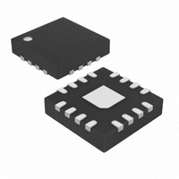
MAX9507ATE+ Maxim Integrated Products, MAX9507ATE+ Datasheet - Page 16

MAX9507ATE+
Manufacturer Part Number
MAX9507ATE+
Description
IC DIRECTDRIVE FILTER AMP 16TQFN
Manufacturer
Maxim Integrated Products
Series
DirectDrive™r
Datasheet
1.MAX9507ATE.pdf
(29 pages)
Specifications of MAX9507ATE+
Applications
Filter
Number Of Circuits
1
-3db Bandwidth
40.7MHz
Slew Rate
35 V/µs
Current - Supply
3.1mA
Current - Output / Channel
82mA
Voltage - Supply, Single/dual (±)
1.7 V ~ 2.63 V
Mounting Type
Surface Mount
Package / Case
16-TQFN Exposed Pad
Supply Current
3.1 mA
Minimum Operating Temperature
- 40 C
Maximum Operating Temperature
+ 125 C
Bandwidth
280 MHz
Maximum Power Dissipation
1250 mW
Mounting Style
SMD/SMT
Supply Voltage (max)
2.625 V
Supply Voltage (min)
1.7 V
For Use With
MAX9507EVKIT+ - KIT EVAL FOR MAX9508MAX9507EVCMAXQU+ - SYSTEM EVAL FOR MAX9507 KIT+MOD
Lead Free Status / RoHS Status
Lead free / RoHS Compliant
The MAX9507 features an I
wire serial interface consisting of a serial-data line (SDA)
and a serial-clock line (SCL). SDA and SCL facilitate
communication between the MAX9507 and the master at
clock rates up to 400kHz. Figure 3 shows the 2-wire inter-
face timing diagram. The master generates SCL and initi-
ates data transfer on the bus. A master device writes data
to the MAX9507 by transmitting a START (S) condition,
the proper slave address with the R/W bit set to 0, fol-
lowed by the register address and then the data word.
Each transmit sequence is framed by a START and a
STOP (P) condition. Each word transmitted to the
MAX9507 is 8 bits long and is followed by an acknowl-
edge clock pulse. A master reads from the MAX9507 by
1.8V DirectDrive Video Filter Amplifier with
Load Detection and Dual SPST Analog Switches
Table 2. Configuration Register (0x00)
* Internal control circuitry prevents the signal path from turning on until the charge pump has been enabled and has settled.
Table 3. Video Load-Detect Register (0x01)
* Read-only bit indicating the load status when the video load-detect circuitry is enabled (ASPEN = 1 or ACPEN = 1). When LCFEN = 1,
reading this bit will clear the LCF flag.
** If SPEN = 0, then the signal path will be automatically enabled when a video load is detected and the charge pump has been
enabled and has settled.
*** If CPEN = 0, then the charge pump will be automatically enabled when a video load is detected.
SMBus is a trademark of Intel Corp.
16
BIT
B7
B3
B1
B0
BIT
B7
B6
B4
B3
B1
B0
______________________________________________________________________________________
ACPEN
LOAD*
LCFEN
ASPEN
NAME
SW2EN
SW1EN
NAME
FLTEN
CPEN
SPEN
STEN
1 = Load detected.
0 = No load detected.
1 = Changes to the video load will trigger LCF to pull low.
0 = Changes to the video load are not reported.
1 = Enable automatic control of the video signal path**.
0 = Disable automatic control of the video signal path.
1 = Enable automatic control of the charge pump***.
0 = Disable automatic control of the charge pump.
1 = Analog switch 2 closed.
0 = Analog switch 2 open.
1 = Analog switch 1 closed.
0 = Analog switch 1 open.
1 = Transparent sync-tip clamp enabled, the input can be DC- or AC-coupled.
0 = Transparent sync-tip clamp disabled, the input must be DC-coupled.
1 = Video filter enabled.
0 = Video filter disabled (bypassed).
1 = Signal path enabled* (SPEN overrides the ASPEN setting).
0 = Signal path disabled.
1 = Charge pump enabled (CPEN overrides the ACPEN setting).
0 = Charge pump disabled.
2
C/SMBus™-compatible, 2-
I
2
C Serial Interface
transmitting the slave address with the R/W bit set to 0,
the register address of the register to be read, a REPEAT-
ED START (Sr) condition, the slave address with the R/W
bit set to 1, followed by a series of SCL pulses. The
MAX9507 transmits data on SDA in sync with the master-
generated SCL pulses. The master acknowledges receipt
of each byte of data. Each read sequence is framed by a
START or REPEATED START condition, an acknowledge
or a not acknowledge, and a STOP condition. SDA oper-
ates as both an input and an open-drain output. A pullup
resistor, typically greater than 500Ω, is required on the
SDA bus. SCL operates as only an input. A pullup resis-
tor, typically greater than 500Ω, is required on SCL if
there are multiple masters on the bus, or if the master in a
single-master system has an open-drain SCL output.
FUNCTION
FUNCTION


