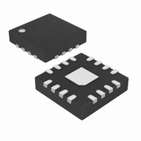
MAX9507ATE+ Maxim Integrated Products, MAX9507ATE+ Datasheet - Page 6

MAX9507ATE+
Manufacturer Part Number
MAX9507ATE+
Description
IC DIRECTDRIVE FILTER AMP 16TQFN
Manufacturer
Maxim Integrated Products
Series
DirectDrive™r
Datasheet
1.MAX9507ATE.pdf
(29 pages)
Specifications of MAX9507ATE+
Applications
Filter
Number Of Circuits
1
-3db Bandwidth
40.7MHz
Slew Rate
35 V/µs
Current - Supply
3.1mA
Current - Output / Channel
82mA
Voltage - Supply, Single/dual (±)
1.7 V ~ 2.63 V
Mounting Type
Surface Mount
Package / Case
16-TQFN Exposed Pad
Supply Current
3.1 mA
Minimum Operating Temperature
- 40 C
Maximum Operating Temperature
+ 125 C
Bandwidth
280 MHz
Maximum Power Dissipation
1250 mW
Mounting Style
SMD/SMT
Supply Voltage (max)
2.625 V
Supply Voltage (min)
1.7 V
For Use With
MAX9507EVKIT+ - KIT EVAL FOR MAX9508MAX9507EVCMAXQU+ - SYSTEM EVAL FOR MAX9507 KIT+MOD
Lead Free Status / RoHS Status
Lead free / RoHS Compliant
1.8V DirectDrive Video Filter Amplifier with
Load Detection and Dual SPST Analog Switches
ELECTRICAL CHARACTERISTICS (continued)
(V
T
Note 1: All devices are 100% production tested at T
Note 2: Voltage gain (A
Note 3: Normal range: charge pump disabled. Extended range: charge pump enabled. In extended range mode, the switch input
Note 4: Flatness is defined as the difference between the maximum and minimum values of on-resistance as measured at the speci-
Note 5: Not production tested, guaranteed by design.
Note 6: t
Note 7: C
6
DIGITAL OUTPUTS (SDA, LCF)
Output Low Voltage
Output High Leakage Current
SERIAL INTERFACE TIMING (Figure 3)
Serial Clock Frequency
Bus Free Time Between STOP
and START Conditions
Hold Time (Repeated) START
Condition
SCL Pulse-Width Low
SCL Pulse-Width High
Setup Time for a Repeated
START Condition
Data Hold Time
Data Setup Time
Bus Capacitance
SDA and SCL Receiving Rise
Time
SDA and SCL Receiving Fall
Time
SDA Transmitting Fall Time
Setup Time for STOP Condition
Pulse Width of Suppressed Spike
MAX
DD
_______________________________________________________________________________________
, unless otherwise noted. Typical values are at T
= +1.8V, GND = 0V, OUT has R
can swing from -0.9V to V
fied voltages.
Figure 1.
ON
B
PARAMETER
is in picofarads.
and t
OFF
are measured from the end of the writing of register 0x00 until COM reaches 90% of the output voltage. See
V
) is a two-point measurement in which the output-voltage swing is divided by the input-voltage swing.
DD
.
L
SYMBOL
t
t
t
t
t
= 150Ω connected to GND, transparent sync-tip clamp enabled, C
HD,STA
HD,DAT
SU,DAT
SU,STO
SU,STA
t
t
t
f
HIGH
V
I
LOW
BUF
t
SCL
C
OH
t
SP
t
t
OL
R
F
F
B
I
V
(Note 7)
(Note 7)
(Note 7)
OL
OUT
A
A
= 3mA
= +25°C. Specifications over temperature are guaranteed by design.
= +25°C.) (Note 1)
= V
DD
CONDITIONS
V
V
V
V
DD
DD
DD
DD
> 2V
< 2V
= 1.7V
= 2.625V
0.1C
0.1C
0.1C
20 +
20 +
20 +
MIN
100
1.3
0.6
1.3
0.6
0.6
0.6
0
0
0
0
B
B
B
1
TYP
= C
2
= 1µF, T
MAX
0.2 x
V
400
900
400
300
300
250
250
0.4
50
DD
1
A
= T
UNITS
kHz
µA
pF
MIN
µs
µs
µs
µs
µs
ns
ns
ns
ns
ns
µs
ns
V
to


